
- Silicon Laboratories, Inc. Clock User Manual

Si53xx-RM
34 Rev. 0.5
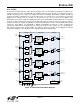
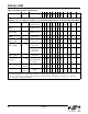
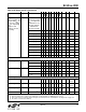
Output Clocks
(CKOUTn—See “8.2. Output Clock Drivers” for Configuring Output Drivers for LVPECL/CML/LVDS/CMOS)
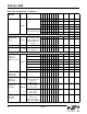
Common Mode V
OCM
LVPECL 100
load line-to-line
V
DD
–
1.42
—V
DD
–
1.25
V
Differential Output
Swing
V
OD
LVPECL 100
load line-to-line
1
1.1 — 1.9 V
PP
Single Ended
Output Swing
V
SE
LVPECL 100
load line-to-line
1
0.5 — 0.93 V
PP
Differential Output
Voltage
CKO
VD
CML 100 load
line-to-line
350 425 500 mV
PP
Common Mode
Output Voltage
CKO
VCM
CML 100 load
line-to-line
—V
DD
– .36
—V
Differential
Output Voltage
CKO
VD
LVDS 100 load
line-to-line
500 700 900 mV
PP
Low swing LVDS
100 load
line-to-line
350 425 500 mV
PP
Common Mode
Output Voltage
CKO
VCM
LVDS 100 load
line-to-line
1.125 1.2 1.275 V
Differential Output
Resistance
CKO
RD
CML, LVPECL,
LVDS, Disabled,
Sleep
170 200 230
Output Voltage Low CKO-
VOLLH
CMOS
——0.4 V
Output Voltage High CKO-
VOHLH
V
DD
= 1.71 V
CMOS
0.8 x
V
DD
—— V
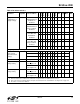
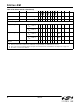
Table 4. DC Characteristics (Continued)
Parameter Symbol Test Condition
Si5316
Si5322
Si5324
Si5325
Si5365
Si5366
Si5367
Si5368
Min Typ Max Units
Notes:
1. Refer to Section 6.7.1 and 8.2.1 for restrictions on output formats for TQFP devices at 3.3 V.
2. This is the amount of leakage that the 3L inputs can tolerate from an external driver. See Figure 55 on page 115.
3. No under- or overshoot is allowed.