
- Silicon Laboratories, Inc. Clock User Manual

Si53xx-RM
Rev. 0.5 81
7.3. Input Clock Configurations (Si5367 and Si5368)
The device supports two input clock configurations based on CK_CONFIG_REG. See "6.5. Frame Synchronization
(Si5366)" on page 70 for additional details.
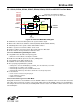
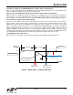
7.4. Input Clock Control
This section describes the clock selection capabilities (manual input selection, automatic input selection, hitless
switching, and revertive switching). The Si5319, Si5327, and Si5375 support only pin-controlled manual clock
selection. Figure 27 and Figure 28 provide top level overviews of the clock selection logic, though they do not
cover wideband or frame sync applications. Register values are indicated by underscored italics. Note that, when
switching between two clocks, LOL may temporarily go high if the clocks differ in frequency by more than 100 ppm.
Figure 27. Si5324, Si5325, Si5326, Si5327, and Si5374 Input Clock Selection
CKIN1
CKIN2
Clock priority logic
CK_PRIORn
0
1
CKSEL_REG
AUTOSEL_REG 0
1
CKSEL_PIN
LOS/FOS
detect
LOS/FOS
detect
LOS/FOS
detect
LOS/FOS
detect
decode
Auto
Manual
Selected
Clock
2
4
CS_CA pin
CK_ACTV_PIN