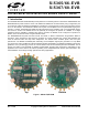
S i 5 3 6 5 / 6 6 - E VB S i 5 3 6 7 / 6 8 - E VB Si5365/66/67/68 E VALUATION B OA RD U SER ’ S G UIDE 1. Introduction The Si5365/66-EVB and Si5367/68-EVB provide platforms for evaluating Silicon Laboratories' Si5365/Si5366 and Si5367/Si5368 Any-Rate Precision Clocks. The Si5365 and Si5366 are controlled directly using configuration pins on the devices, while the Si5367 and Si5368 are controlled by a microprocessor or MCU (microcontroller unit) via an I2C or SPI interface.
Si5365/66-EVB Si5367/68-EVB Alarms 0.6 ps rms typ 30 kHz–1.3 MHz Y N LOS, FOS 14 x 14 100-QFN Si5367 4 5 I2C or SPI 10 to 710 10 to 1400 0.6 ps rms typ 30 kHz–1.3 MHz Y N LOS, FOS 14 x 14 100-QFN Input Freq (MHz) Control Package Hitless Switching 19 to 1050 Prog. Loop BW 15 to 707 Jitter Generation (12 kHz–20 MHz) Pin Output Freq (MHz) 5 # Clock Outputs 4 # Clock Inputs Si5365 Device PN Clock Mult. Table 1.
Si5365/66-EVB Si5367/68-EVB 4. Si5365/66-EVB and Si5367/68-EVB Quick Start 1. Install the Precision Clock EVB Driver. (This must be installed before the EVB is connected to the PC via the USB cable.) For details, see Section "7.EVB Software Installation" on page 11. 2. Install the Precision Clock EVB Software. (Assumes that Microsoft .NET Framework 1.1 is already installed.) 3. Connect the two power supplies to the EVB. One is 3.3 V and the other is either 1.8 or 2.5 V. The DUT is powered by the 1.8/2.
Si5365/66-EVB Si5367/68-EVB Ext RefClk SPI bus CKOUT1 USB MCU Terminate Input SMAs Reset switch CKOUT2 Si536x CKOUT3 Output SMAs CKOUT4 LEDs FSOUT +3.3 V 1.8 to 3.3 V DUT PWR +1.8 V Vreg ss CPLD SPI, I2C signals reg addr SPI bus Jumper status signals Headers Control signals Figure 2. Si536x TQFP Block Diagram 5.3. Si536x Input and Output Clocks The Si536x has four differential inputs that are ac terminated to 50 Ω and then ac coupled to the part.
Si5365/66-EVB Si5367/68-EVB Table 2. Reference Input Mode Mode Xtal1 38.88 MHz Ext Ref2 Wide Band Input 1 NC3 J1 NC Input 2 NC J2 NC C39 NOPOP4 install install C22 NOPOP install NOPOP R50 NOPOP NOPOP install R28 install NOPOP NOPOP RATE0 M — H RATE1 M — H Notes: 1. Xtal is 114.285 MHz 3rd overtone. 2. For external reference frequencies and RATE pin settings, see the Any-Rate Precision Clock Family Reference Manual. 3. NC—no connect. 4. NOPOP—do not install this component.
Si5365/66-EVB Si5367/68-EVB 5.5. MCU The MCU communicates with the PC over USB so that PC resident software can be used to control and monitor the Si536x. The USB connector is J6 and the debug port, by which the MCU is flashed, is J31. The reset switch, SW1, resets the MCU, but not the CPLD. The MCU is a self-contained USB master and runs all of the code required to control and monitor the Si536x, both in the MCU mode and in the pin-controlled modes.
Si5365/66-EVB Si5367/68-EVB 6. Connectors and LEDs 6.1. LEDs There are sixteen LEDs on the board which provide a quick and convenient means of determining board status. Table 3. LED Status and Description LED Color Label LED Color Label D1 green 3.
Si5365/66-EVB Si5367/68-EVB 6.2. User Jumpers and Headers. Use Figure 4 to locate the jumpers described in Tables 4, 5, 6, and 7: Ext Ref, J1, J2 J8 J14 C22 R24, R28, C22 on top; R50, R51, R52, C39 on bot J18 J17 J25, R36 J22 Figure 4. Connectors, Jumper Header Locations J25 assists in measuring the Any-Rate Precision Clock current draw. If J25 is to be used, R36 should be removed. 8 Rev. 0.
Si5365/66-EVB Si5367/68-EVB J14 is a three-pin by ten header that is used to establish input levels for the pin controlled two-level inputs using jumper plugs. It also provides a means of externally driving the two-level input signals: Table 4. Two-Level Input Jumper Header, J14 J36 Pin Comment J14.1B CS0_C3A CS0 J14.2B CS1_C4A CS1 J14.3B INC J14.4B DEC J14.5B — not used J14.6B — not used J14.7B DSBL34 J14.8B FS_ALIGN J14.9B FS_SW J14.
Si5365/66-EVB Si5367/68-EVB Table 6. External Serial Port Connector, J22 J38 Pin J22.1 SDA_SDO J22.3 SCL_SCLK J22.5 SDI J22.7 A2_SS J22.9 DUT_RST_B Comment reset J17 is a three-pin by twenty header that is used to establish input levels for the pin controlled three-level inputs using jumper plugs. It also provides a means of externally driving the three-level input signals. Table 7. Three-Level Input Jumper Headers, J17 J39 Pin Comment J17.1B CMODE J17.2B AUTOSEL J17.
Si5365/66-EVB Si5367/68-EVB 7. EVB Software Installation The following sections describe how to install the EVB software. Note: These programs can control any of the Any-Rate Precision Clock devices including the Si5316, Si532x, and Si536x devices. This software can be installed once per PC and used for all available Precision Clock EVBs. 7.1. PC System Requirements Microsoft Windows 2000 or Windows XP USB 1.1 or USB 2.
Si5365/66-EVB Si5367/68-EVB 7.4. Precision Clock EVB Software Installation To install: 1. Navigate to the "PrecisionClockEVBSoftware" directory. 2. Double-click on the Setup.exe file 3. Follow the steps in the wizard to install the program. Note: Use the default installation location for best results. 4. After the installation is complete, click on Start→Programs→Silicon Laboratories→Precision Clock EVB Software. Select one of the programs to control the EVB. 5.
49.9 R61 J30 J33 SMA_EDGE 1 CKIN4- SMA_EDGE 1 J38 SMA_EDGE 1 DBL2_BY SDA_SDO_BWSEL1 SCL_SCLK_BWSEL0 SDI_FRQSEL3 A2_SS_FRQSEL2 A1_FRQSEL1 A0_FRQSEL0 CK_CONF FRQTBL CMODE DUT_RST_B FS_SW FS_ALIGN FOS_CTL AUTOSEL INC DEC DIV34_1 DIV34_0 49.9 C42 100N R54 100N R53 R59 49.9 49.9 C55 C53 49.9 49.9 C50 C47 100N 100N J37 R57 R56 100N 100N R55 49.9 C61 C58 100N 100N R60 49.
Rev. 0.4 DUT_PWR 10 R15 0 ohm R10 R19 0 ohm R14 10 C8 1UF VCCAUX TMS TDI TDO TCK V3P3 C23 1UF 1 2 3 4 5 6 SMT J32 JTAG connector V3P3 1 2 3 5 83 47 48 45 FB Vreg Out C21 100N TPS76201 Gnd EN In U4 XC2C128 VCCAUX TDO TMS TCK TDI U10B 4 5 C20 10NF C14 1UF R16 66.5 R45 113 V1P8 + C12 100N C7 33UF 1.
MISO SCLK CPLD_SPARE10 CPLD_SPARE9 CPLD_SPARE8 CPLD_SPARE7 CPLD_SPARE6 CPLD_SPARE5 CPLD_SPARE4 CPLD_SPARE2 CPLD_SPARE1 SS_CPLD_B W CS D Clk U5 7 3 1 5 6 49.9 49.9 49.9 M95040 HOLD EEPROM Q MOSI CPLD_IRQ MCU_SPARE1 MCU_SPARE2 2 8 Vcc Vss 4 C38 100N R17 R41 R11 R42 49.9 R46 10k 10k R4 J34 10_M_Header_SMT Spares C4 1UF C1 100N 46 45 44 43 42 41 40 39 6 5 4 3 2 1 48 47 P1.0 P1.1 P1.2 P1.3 P1.4 P1.5 P1.6 P1.7 P0.0 P0.1 P0.2 P0.3 P0.4 P0.5 P0.6 P0.
1 2 3 MCU_LED1 MCU_LED2 MCU_LED3 CPLD_LED0 CPLD_LED1 CPLD_LED2 R69 1K EVB main power Phoenix_4_screw 3.3V 3.
J22 9 7 5 3 1 Rev. 0.4 R64 NOPOP 0 ohm R62 R82x4 10 R26 R22 1.5K NOPOP DUT_PWR install for I2C R25 1.5K NOPOP R72 10k J17 R70 10k 1C 2C 3C 4C 5C 6C 7C 8C 9C 10C 11C 12C 13C 14C 15C 16C 17C 18C 19C 20C 20x3_M_HDR_SMT 20A 20B 19A 19B 18A 18B 17A 17B 16A 16B 15A 15B 14A 14B 13A 13B 12A 12B 11A 11B 10A 10B 9A 9B 8A 8B 7A 7B 6A 6B 5A 5B 4A 4B 3A 3B 2A 2B 1A 1B R58 100 DUT_PWR Figure 9. Serial Port, 3L Inputs Notes: 2. NOPOP for Si5365 and Si55366.
Si5365/66-EVB Si5367/68-EVB 9. Bill of Materials Table 9.
Si5365/66-EVB Si5367/68-EVB Table 9. Si536x Bill of Materials (Continued) Item Qty Reference Part Mfgr MfgrPartNum 31 5 R8,R10,R14,R26,R39 10 Venkel CR0603-16W-10R0FT 33 9 R15,R19,R28,R29,R31,R36,R38, R48,R73 0 ohm Venkel CR0603-16W-000T 34 1 R16 66.5 Venkel CR0603-16W-66R5FT 36 2 R27,R58 100 Venkel CR0603-16W-1000FT 37 4 R32,R33,R34,R35 R150x4 Panasonic EXB-38V151JV 39 1 R45 113 Venkel CR0603-16W-1130FT 40 1 R49 82.
Si5365/66-EVB Si5367/68-EVB 10. Layout Figure 10. Silkscreen Top Figure 11. Layer 1 20 Rev. 0.
Si5365/66-EVB Si5367/68-EVB Figure 12. Layer 2, Ground Plane Figure 13. Layer 3 Rev. 0.
Si5365/66-EVB Si5367/68-EVB Figure 14. Layer 4, 3.3 V Power Figure 15. Layer 5 22 Rev. 0.
Si5365/66-EVB Si5367/68-EVB Figure 16. Layer 6, DUT Power Figure 17. Layer 7, Ground Plane Rev. 0.
Si5365/66-EVB Si5367/68-EVB Figure 18. Layer 8 Figure 19. Silkscreen Bottom 24 Rev. 0.
Si5365/66-EVB Si5367/68-EVB APPENDIX—POWERUP AND FACTORY DEFAULT SETTINGS For the Si5367/68-EVB, the power up settings are as follows: 19.44 MHz input on either CKIN1, CKIN3 or CKIN4 CKIN2 is not used because of free run mode 155.52 MHz output on CKOUT1 and CKOUT2 622.08 MHz output on CKOUT3 and CKOUT4 311.04 MHz output on CKOUT5 Loop BW of 70 Hz LVEPCL outputs for CKIN1, CKIN2, CKIN3 and CKIN4 For the Si5365/66-EVB, the factory jumper settings are as follows: For J17: Silkscreen Pin Jumper — J17.
Si5365/66-EVB Si5367/68-EVB For J14: Pin Pin Jumper CS0_C3A J14.1B none CS1_C4A J14.2B none INC J14.3B none DEC J14.4B none — J14.5B none — J14.6B none DBL34 J14.7B none CKOUT3, CKOUT 4 enabled FS_ALIGN J14.8B none no FS alignment FS_SW J14.9B none CKIN3, CKIN 4 not LOS inputs CK_CONF J14.10B none no FS out alignment 26 Comment Rev. 0.
Si5365/66-EVB Si5367/68-EVB DOCUMENT CHANGE LIST Revision 0.2 to Revision 0.3 Updated "5.3.Si536x Input and Output Clocks" on page 4. Updated "5.5.MCU" on page 6. Added "Appendix—Powerup and Factory Default Settings" on page 25. Revision 0.3 to Revision 0.4 Updated for free run mode. Rev. 0.
Si5365/66-EVB Si5367/68-EVB CONTACT INFORMATION Silicon Laboratories Inc. 400 West Cesar Chavez Austin, TX 78701 Tel: 1+(512) 416-8500 Fax: 1+(512) 416-9669 Toll Free: 1+(877) 444-3032 Email: clockinfo@silabs.com Internet: www.silabs.com The information in this document is believed to be accurate in all respects at the time of publication but is subject to change without notice.