
- Silicon Laboratories, Inc. Clock User Manual

Si53xx-RM
24 Rev. 0.5
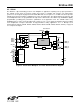
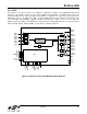
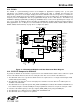
3.8. Si5327
The Si5327 is a jitter-attenuating precision clock multiplier for applications requiring sub 1 ps jitter performance.
The Si5327 accepts dual clock inputs ranging from 2 kHz to 710 MHz and generates two independent,
synchronous clock outputs ranging from 2 kHz to 808 MHz. The device provides virtually any frequency translation
combination across this operating range. The Si5327 input clock frequency and clock multiplication ratios are
programmable through an I
2
C or SPI interface. The DSPLL loop bandwidth is digitally programmable, providing
jitter performance optimization at the application level. The Si5327 features loop bandwidth values as low as 4 Hz.
Operating from a single 1.8, 2.5, or 3.3 V supply, the Si5327 is ideal for providing clock multiplication and jitter
attenuation in high-performance timing applications. See "7. Microprocessor Controlled Parts (Si5319, Si5324,
Si5325, Si5326, Si5327, Si5367, Si5368, Si5369, Si5374, Si5375)" on page 76 for a complete description.
Figure 8. Si5327 Clock Multiplier and Jitter Attenuator Block Diagram
÷ N31
INT_C1B
Xtal or Refclock
÷ NC1
÷ NC2
Signal
Detect
VDD
GND
C2B
0
1
f
3
CKOUT_2 +
CKOUT_2 –
CKOUT_1 +
CKOUT_1 –
/
/
2
2
1
0
1
0
f
OSC
RATE[1:0]
LOL
CS_CA
SDA_SDO
INC
DEC
RST
SCL
Control
SDI
A[2]/SS
A[1:0]
XAXB
CMODE
CKIN_1 +
CKIN_1 –
2
2
CKIN_2 +
CKIN_2 –
÷ N32
0
1
3
BYPASS
÷ N2
DSPLL
÷ N1_HS
DSPLL
®