
Specifications


C8051F330/1
Rev. 1.1 101
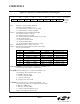
Figure 11.3. FLKEY: FLASH Lock and Key Register
Bits7-0: FLKEY: FLASH Lock and Key Register
Write:
This register provides a lock and key function for FLASH erasures and writes. FLASH writes and
erases are enabled by writing 0xA5 followed by 0xF1 to the FLKEY register. FLASH writes and
erases are automatically disabled after the next write or erase is complete. If any writes to FLKEY are
performed incorrectly, or if a FLASH write or erase operation is attempted while these operations are
disabled, the FLASH will be permanently locked from writes or erasures until the next device reset.
If an application never writes to FLASH, it can intentionally lock the FLASH by writing a non-0xA5
value to FLKEY from software.
Read:
When read, bits 1-0 indicate the current FLASH lock state.
00: FLASH is write/erase locked.
01: The first key code has been written (0xA5).
10: FLASH is unlocked (writes/erases allowed).
11: FLASH writes/erases disabled until the next reset.
R/W R/W R/W R/W R/W R/W R/W R/W Reset Value
00000000
Bit7 Bit6 Bit5 Bit4 Bit3 Bit2 Bit1 Bit0
SFR Address:
0xB7
Figure 11.4. FLSCL: FLASH Scale Register
Bit7: FOSE: FLASH One-shot Enable
This bit enables the FLASH read one-shot. When the FLASH one-shot disabled, the FLASH sense
amps are enabled for a full clock cycle during FLASH reads. At system clock frequencies below
10 MHz, disabling the FLASH one-shot will increase system power consumption.
0: FLASH one-shot disabled.
1: FLASH one-shot enabled.
Bits6-0: RESERVED. Read = 0. Must Write 0.
R/W R/W R/W R/W R/W R/W R/W R/W Reset Value
FOSE Reserved Reserved Reserved Reserved Reserved Reserved Reserved 10000000
Bit7 Bit6 Bit5 Bit4 Bit3 Bit2 Bit1 Bit0
SFR Address:
0xB6