
Specifications


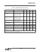


C8051F330/1
Rev. 1.1 23
1.7. 10-Bit Analog to Digital Converter
The C8051F330/1 devices include an on-chip 10-bit SAR ADC with a 16-channel differential input multiplexer. With
a maximum throughput of 200
ksps, the ADC offers true 10-bit linearity with an INL and DNL of ±1LSB. The ADC
system includes a configurable analog multiplexer that selects both positive and negative ADC inputs. Ports0-1 are
available as an ADC inputs; additionally, the on-chip Temperature Sensor output and the power supply voltage
(VDD) are available as ADC inputs. User firmware may shut down the ADC to save power.
Conversions can be started in six ways: a software command, an overflow of Timer 0, 1, 2, or 3, or an external con-
vert start signal. This flexibility allows the start of conversion to be triggered by software events, a periodic signal
(timer overflows), or external HW signals. Conversion completions are indicated by a status bit and an interrupt (if
enabled). The resulting 10-bit data word is latched into the ADC data SFRs upon completion of a conversion.
Window compare registers for the ADC data can be configured to interrupt the controller when ADC data is either
within or outside of a specified range. The ADC can monitor a key voltage continuously in background mode, but not
interrupt the controller unless the converted data is within/outside the specified range.
Figure 1.9. 10-Bit ADC Block Diagram
ADC0CF
AD0LJST
AD0SC0
AD0SC1
AD0SC2
AD0SC3
AD0SC4
10-Bit
SAR
ADC
REF
SYSCLK
ADC0H
32
ADC0CN
AD0CM0
AD0CM1
AD0CM2
AD0WINT
AD0BUSY
AD0INT
AD0TM
AD0EN
Timer 0 Overflow
Timer 2 Overflow
Timer 1 Overflow
Start
Conversion
000 AD0BUSY (W)
VDD
ADC0LTH
18-to-1
AMUX
AD0WINT
Temp
Sensor
18-to-1
AMUX
VDD
P0.0
P0.7
001
010
011
100
CNVSTR Input
Window
Compare
Logic
P1.0
P1.7
GND
P0.0
P0.7
P1.0
P1.7
101 Timer 3 Overflow
ADC0LTL
ADC0GTH ADC0GTL
ADC0L
AMX0P
AMX0P4
AMX0P3
AMX0P2
AMX0P1
AMX0P0
AMX0N
AMX0N4
AMX0N3
AMX0N2
AMX0N1
AMX0N0
(+)
(-)
VREF