
Specifications


C8051F330/1
Rev. 1.1 79
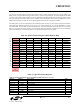
Figure 9.5. SP: Stack Pointer
Bits7-0: SP: Stack Pointer.
The Stack Pointer holds the location of the top of the stack. The stack pointer is incremented before
every PUSH operation. The SP register defaults to 0x07 after reset.
R/W R/W R/W R/W R/W R/W R/W R/W Reset Value
00000111
Bit7 Bit6 Bit5 Bit4 Bit3 Bit2 Bit1 Bit0 SFR Address:
0x81
Figure 9.6. PSW: Program Status Word
Bit7: CY: Carry Flag.
This bit is set when the last arithmetic operation resulted in a carry (addition) or a borrow (subtrac-
tion). It is cleared to logic 0 by all other arithmetic operations.
Bit6: AC: Auxiliary Carry Flag
This bit is set when the last arithmetic operation resulted in a carry into (addition) or a borrow from
(subtraction) the high order nibble. It is cleared to logic 0 by all other arithmetic operations.
Bit5: F0: User Flag 0.
This is a bit-addressable, general purpose flag for use under software control.
Bits4-3: RS1-RS0: Register Bank Select.
These bits select which register bank is used during register accesses.
Bit2: OV: Overflow Flag.
This bit is set to 1 under the following circumstances:
• An ADD, ADDC, or SUBB instruction causes a sign-change overflow.
• A MUL instruction results in an overflow (result is greater than 255).
• A DIV instruction causes a divide-by-zero condition.
The OV bit is cleared to 0 by the ADD, ADDC, SUBB, MUL, and DIV instructions in all other cases.
Bit1: F1: User Flag 1.
This is a bit-addressable, general purpose flag for use under software control.
Bit0: PARITY: Parity Flag.
This bit is set to logic 1 if the sum of the eight bits in the accumulator is odd and cleared if the sum is
even.
R/W R/W R/W R/W R/W R/W R/W R Reset Value
CY AC F0 RS1 RS0 OV F1 PARITY 00000000
Bit7 Bit6 Bit5 Bit4 Bit3 Bit2 Bit1 Bit0 SFR Address:
(bit addressable)
0xD0
RS1 RS0 Register Bank Address
0 0 0 0x00 - 0x07
0 1 1 0x08 - 0x0F
1 0 2 0x10 - 0x17
1 1 3 0x18 - 0x1F