
User's Guide


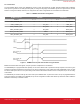

Table Of Contents
- 1. WFM200 Pinout
- 2. Device Configuration
- 3. Features Description
- 4. Power Supplies
- 5. Application Schematic Recommendations
- 6. Typical Application Schematics
- 7. Layout Recommendations
- 7.1 Generic RF Layout Considerations
- 7.2 GND and RF Pads Including the Diversity Port and External Antennas
- 7.3 Module Antenna
- 7.3.1 Small Board Size Recommendations for Good RF Performance
- 7.3.2 Extended X Dimension Recommendation for Good RF Performance
- 7.3.3 Y Dimension (65 to 80 mm) Recommendation for Good RF Performance
- 7.3.4 Y Dimension (80 mm or Larger) Recommendation for Good RF Performance
- 7.3.5 WFM200 Portion One Corner Bias with 3 mm Metal Keep-Outs
- 7.3.6 Recommended Antenna Loop Trace Capacitor Values
- 7.4 WFM200 Reference Evaluation Board
- 8. Recommendations for Certification
- 9. Package Outline
- 10. Integral Antenna Loop and Keep-Out Required Dimensions
- 11. Recommended PCB Land Pattern

5. Application Schematic Recommendations
5.1 Power Supplies – Schematics
Care should be taken that the VDD_PA supply source is capable of supplying enough current for the load peaks of the power amplifier
(which can go momentarily up to 200 mA), so it is recommended to select a regulator capable of supplying 300 mA. The peaks can be
very fast, and the power supply for the module should be capable of reacting to load changes within 5 μs.
External high-frequency bypass capacitors are not needed because the module contains the required supply filter capacitors. However,
care should be taken to prevent strong switching noise from being superimposed on the supply lines. Such noise can be generated, for
example, by the onboard charge pump converters used in RS232 level shifters, in which case it is recommended to place series ferrite
and decoupling capacitors with proper SRF at the switching noise frequencies on the supply lines connected. Silicon Labs reference
expansion board design with the WFM200 SiP module utilizes a series ferrite with a 10 μF decoupling capacitor between the external
power regulator and SiP.
Note that there is a total of about 2.3 μF of low ESR ceramic capacitors inside the module connected directly on the supply input. When
using external regulators to generate regulated supplies for the module, the stability of the regulator with the low ESR provided by these
capacitors should be checked. Some low-drop linear regulators and some older switched mode regulators are not stable when ceramic
output capacitors are used. The data sheet of the regulator typically lists recommendations concerning suitable capacitors, including
data on ESR range and/or stability curves. A regulator should include the statement “stable with ceramic capacitors”.
5.2 RF Ports – Schematics
When using the module with the integrated antenna or an antenna external to the module, whether they are connectorized off-the-shelf
antennas or PCB trace antennas, antenna impedance must be well matched to 50 Ω to reduce distortion in the module power amplifier
because of the impedance mismatch. The matching should be verified in the final enclosure, and it is recommended to reserve SMD
placeholders for external antenna tuning.
The suggested external antenna matching structure is a 3-element PI network. The optimum load impedance for each RF port is 50 Ω,
so externally, only the antenna matching components may be required.
When using the integrated module antenna (with its required external GND loop trace on the top layer and copper clearance area ap-
plied on each layer), the RF_1 port needs to be connected to the 2G4ANT_IN port while externally only a capacitor is required on the
antenna loop trace (C_ANT) to the GND.
Unused RF port must be terminated to ground with a resistor between 47 and 51 Ω.
• External antennas used with the Single Modular Transmitter are required to meet these specifications. For reference impedance of
50 Ω, the VSWR must be less than or equal to 2:1 (which is the same as Return Loss higher than 9.5 dB), over the allowed operat-
ing frequency range for all operating conditions and production variations.
• The integral antenna on the reference board nominally achieves 18 dB return loss from 2412 MHz to 2462 MHz with reference impe-
dance of 50 Ω. Production tolerance and variations over operating conditions of the main board can degrade this to 12 dB return
loss. Production tolerance and variations over operating conditions of WFM200 module can further degrade up to VSWR = 2:1.
• If the hardware design guide is not properly followed, the resulting VSWR may be higher than 2:1 over operating conditions, which
would require Tx Output Power to be reduced using PDS file Back Off, and possibly agency approval.
UG395: WFM200 Hardware Design User's Guide
Application Schematic Recommendations
silabs.com | Building a more connected world. Preliminary Rev. 0.1 | 10