
User's Guide


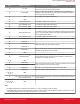
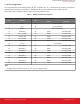

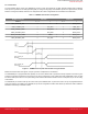

Table Of Contents
- 1. WFM200 Pinout
- 2. Device Configuration
- 3. Features Description
- 4. Power Supplies
- 5. Application Schematic Recommendations
- 6. Typical Application Schematics
- 7. Layout Recommendations
- 7.1 Generic RF Layout Considerations
- 7.2 GND and RF Pads Including the Diversity Port and External Antennas
- 7.3 Module Antenna
- 7.3.1 Small Board Size Recommendations for Good RF Performance
- 7.3.2 Extended X Dimension Recommendation for Good RF Performance
- 7.3.3 Y Dimension (65 to 80 mm) Recommendation for Good RF Performance
- 7.3.4 Y Dimension (80 mm or Larger) Recommendation for Good RF Performance
- 7.3.5 WFM200 Portion One Corner Bias with 3 mm Metal Keep-Outs
- 7.3.6 Recommended Antenna Loop Trace Capacitor Values
- 7.4 WFM200 Reference Evaluation Board
- 8. Recommendations for Certification
- 9. Package Outline
- 10. Integral Antenna Loop and Keep-Out Required Dimensions
- 11. Recommended PCB Land Pattern

1. WFM200 Pinout
WFM200 is a 6.5 x 6.5 mm LGA module. The diagram below describes the pinout (top view).
Figure 1.1. WFM200 Pinout
Table 1.1. WFM200 Pin Description
Pin # WFM200 Pin Name Description
1 GND
2
2G4ANT_IN, or No Connect on OPN
with no integral antenna
Embedded 2.4 GHz antenna port. To use the antenna, connect this pin to
RF_1.
3 RF_1
50 Ω RF_1 input/output port. If not used, this pin should be connected to
GND through a 50 Ω resistor.
4, 5, 6, 7, 8 GND
9 RF_2
50 Ω RF_2 input/output port. If not used, this pin should be connected to
GND through a 50 Ω resistor.
10 VDD_PA Power supply for the power amplifier.
11 GND
12 RESETn RESET pin, active Low.
13 GPIO/WUP This pin can be used to wake-up the device from sleep mode or as a GPIO.
14 GPIO/PTA_TX_CONF
As part of PTA interface, these pins can be used to manage co-existence
with another 2.4 GHz radio or can be used as a GPIO.
15 GPIO/PTA_RF_ACT
16 GPIO/PTA_STATUS
17 GPIO/PTA_FREQ
UG395: WFM200 Hardware Design User's Guide
WFM200 Pinout
silabs.com | Building a more connected world. Preliminary Rev. 0.1 | 3