
User's Guide

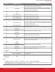
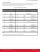

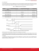

Table Of Contents
- 1. WFM200 Pinout
- 2. Device Configuration
- 3. Features Description
- 4. Power Supplies
- 5. Application Schematic Recommendations
- 6. Typical Application Schematics
- 7. Layout Recommendations
- 7.1 Generic RF Layout Considerations
- 7.2 GND and RF Pads Including the Diversity Port and External Antennas
- 7.3 Module Antenna
- 7.3.1 Small Board Size Recommendations for Good RF Performance
- 7.3.2 Extended X Dimension Recommendation for Good RF Performance
- 7.3.3 Y Dimension (65 to 80 mm) Recommendation for Good RF Performance
- 7.3.4 Y Dimension (80 mm or Larger) Recommendation for Good RF Performance
- 7.3.5 WFM200 Portion One Corner Bias with 3 mm Metal Keep-Outs
- 7.3.6 Recommended Antenna Loop Trace Capacitor Values
- 7.4 WFM200 Reference Evaluation Board
- 8. Recommendations for Certification
- 9. Package Outline
- 10. Integral Antenna Loop and Keep-Out Required Dimensions
- 11. Recommended PCB Land Pattern

Pin # WFM200 Pin Name Description
18 LP_CLK
Low Power clock input. This pin is typically connected to the 32 kHz clock. If
not used, the pin should be connected to GND.
19 GPIO/WIRQ
This pin can be used as an IRQ from WFM200 to host to indicate that a
message or data should be read or can be used as a GPIO if the WIRQ is
done using SDIO_DAT1/SPI_WIRQ.
20 VDD Power supply for the digital and RF parts.
21 GND
22 SDIO_CLK/SPI_CLK Host interface: SDIO_CLK or SPI_CLK.
23 SDIO_CMD/SPI_MOSI Host interface: SDIO_CMD or SPI_MOSI.
24 SDIO_DAT0/SPI_MISO Host interface: SDIO_DAT0 or SPI_MISO.
25 SDIO_DAT1/SPI_WIRQ Host interface: SDIO_DAT1 or WIRQ.
26 SDIO_DAT2/HIF_SEL
Host interface selection: Used to select the host interface during reset rising
edge. If Low, selects SPI interface. When High, selects SDIO interface and
this pin becomes SDIO_DAT2.
27 SDIO_DAT3/SPI_CSn Host interface: SDIO_DAT3 or SPI_CSn.
28 VDD_IO Power supply for I/Os.
29 GPIO/FEM_1
These pins can be used for dynamic control of an external front-end module
(FEM); otherwise, they can be used as a GPIO.
30 GPIO/FEM_2
31 GPIO/FEM_3
32 GPIO/FEM_4
This pin can be used for dynamic control of an external Power Amplifier;
otherwise, this pin can be used as a GPIO.
33 GND
34
GPIO/FEM_PDET
(2)
This pin can be used as an analog input to be connected to a Power Ampli-
fier Vdet output whenever an external Power amplifier or a FEM is used.
Otherwise, it can be used as a GPIO.
35, 36 GND
37 GPIO/FEM_6
These pins can be used for dynamic control of an external front-end module
(FEM); otherwise, this can be used as a GPIO.
38 GPIO/FEM_5
39 RESERVE_1 Reserved. For normal operation, this pin must be grounded.
40 RESERVE_2 Reserved. Leave this pin unconnected.
41, 42, 43, 44,
45, 46,
GND
47
ANT_LOOP, or No Connect on OPN
with no integral antenna
To use the embedded antenna, connect this pin to GND through the anten-
na loop capacitor.
48, 49, 50, 51,
52, 53, 54, 55,
56, 57, 58
GND
Note:
1. All digital pins (GPIO/xx, host interface pins, RESETn, LP_CLK) are referred to VDD_IO voltage.
2. GPIO/FEM_PDET requires special care because it refers to VDD_IO voltage when configured as a GPIO. However,when config-
ured as FEM_PDET, this pin is an analog input pin with a 0 to 1.2 V range.
UG395: WFM200 Hardware Design User's Guide
WFM200 Pinout
silabs.com | Building a more connected world. Preliminary Rev. 0.1 | 4