
User's Guide

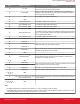

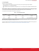

Table Of Contents
- 1. WFM200 Pinout
- 2. Device Configuration
- 3. Features Description
- 4. Power Supplies
- 5. Application Schematic Recommendations
- 6. Typical Application Schematics
- 7. Layout Recommendations
- 7.1 Generic RF Layout Considerations
- 7.2 GND and RF Pads Including the Diversity Port and External Antennas
- 7.3 Module Antenna
- 7.3.1 Small Board Size Recommendations for Good RF Performance
- 7.3.2 Extended X Dimension Recommendation for Good RF Performance
- 7.3.3 Y Dimension (65 to 80 mm) Recommendation for Good RF Performance
- 7.3.4 Y Dimension (80 mm or Larger) Recommendation for Good RF Performance
- 7.3.5 WFM200 Portion One Corner Bias with 3 mm Metal Keep-Outs
- 7.3.6 Recommended Antenna Loop Trace Capacitor Values
- 7.4 WFM200 Reference Evaluation Board
- 8. Recommendations for Certification
- 9. Package Outline
- 10. Integral Antenna Loop and Keep-Out Required Dimensions
- 11. Recommended PCB Land Pattern

2. Device Configuration
The configuration linked to the hardware platform (RF pins, configurable pins, etc.) is achieved through firmware by downloading a
dedicated binary file (a PDS file, which stands for "Platform Data Set") just after firmware download and before operation.
More details on device configuration will be provided in an upcoming application note.
Table 2.1. WFM200 Pin Status and Impedance
Pin # Pin Name I/O
Configuration
Reset
1
After Boot
3 RF_1 I/O 50 Ω at 2442 MHz
9 RF_2 I/O 50 Ω at 2442 MHz
12 RESETn I 43 kΩ pull-up resistor
13 GPIO/WUP I/O tristate according to PDS
14 PTA_TX_CONF I/O tristate according to PDS
15 PTA_RF_ACT I/O tristate according to PDS
16 PTA_STATUS I/O tristate according to PDS
17 PTA_FREQ I/O tristate according to PDS
18 LP_CLK I no pull resistor
19 GPIO_WIRQ I/O tristate according to PDS
29 GPIO/FEM_1 I/O tristate according to PDS
30 GPIO/FEM_2 I/O tristate according to PDS
31 GPIO/FEM_3 I/O tristate according to PDS
32 GPIO/FEM_4 I/O tristate according to PDS
34 GPIO/FEM_DET I/O tristate according to PDS
37 GPIO/FEM_6 I/O tristate according to PDS
38 GPIO/FEM_5 I/O tristate according to PDS
Note:
1. All digital I/Os are in tristate except pin LP_CLK, which is configured as input.
UG395: WFM200 Hardware Design User's Guide
Device Configuration
silabs.com | Building a more connected world. Preliminary Rev. 0.1 | 5