
User's Guide


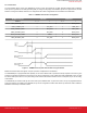

Table Of Contents
- 1. WFM200 Pinout
- 2. Device Configuration
- 3. Features Description
- 4. Power Supplies
- 5. Application Schematic Recommendations
- 6. Typical Application Schematics
- 7. Layout Recommendations
- 7.1 Generic RF Layout Considerations
- 7.2 GND and RF Pads Including the Diversity Port and External Antennas
- 7.3 Module Antenna
- 7.3.1 Small Board Size Recommendations for Good RF Performance
- 7.3.2 Extended X Dimension Recommendation for Good RF Performance
- 7.3.3 Y Dimension (65 to 80 mm) Recommendation for Good RF Performance
- 7.3.4 Y Dimension (80 mm or Larger) Recommendation for Good RF Performance
- 7.3.5 WFM200 Portion One Corner Bias with 3 mm Metal Keep-Outs
- 7.3.6 Recommended Antenna Loop Trace Capacitor Values
- 7.4 WFM200 Reference Evaluation Board
- 8. Recommendations for Certification
- 9. Package Outline
- 10. Integral Antenna Loop and Keep-Out Required Dimensions
- 11. Recommended PCB Land Pattern

3. Features Description
3.1 WFM200 RF Ports
WFM200 has two Tx/Rx RF ports named RF_1 (pin 3) and RF_2 (pin 9). RF_1 and RF_2 have internal low-pass filtering and RF impe-
dance matching components to 50 Ω in the 2.4 GHz band of operation. Any of the RF ports can be used in a similar way. However,
note that RF_2 output power is around 1 dB lower than that of RF_1. Several configurations for the RF part are possible, as described
below:
• Single antenna: For this use case, any RF pin can be used.
• Antenna diversity without external FEM: In this case, both RF_1 and RF_2 ports are connected to their respective antennas and,
over time, the WFM200 selects the antenna that provides the best budget link to optimize performance, range, and throughput.
• Use of an external Front-End Module (FEM): In this case, one port is used for Tx and the other for Rx.
This RF configuration is set with the PDS file.
UG395: WFM200 Hardware Design User's Guide
Features Description
silabs.com | Building a more connected world. Preliminary Rev. 0.1 | 6