
User's Guide

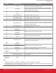

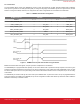

Table Of Contents
- 1. WFM200 Pinout
- 2. Device Configuration
- 3. Features Description
- 4. Power Supplies
- 5. Application Schematic Recommendations
- 6. Typical Application Schematics
- 7. Layout Recommendations
- 7.1 Generic RF Layout Considerations
- 7.2 GND and RF Pads Including the Diversity Port and External Antennas
- 7.3 Module Antenna
- 7.3.1 Small Board Size Recommendations for Good RF Performance
- 7.3.2 Extended X Dimension Recommendation for Good RF Performance
- 7.3.3 Y Dimension (65 to 80 mm) Recommendation for Good RF Performance
- 7.3.4 Y Dimension (80 mm or Larger) Recommendation for Good RF Performance
- 7.3.5 WFM200 Portion One Corner Bias with 3 mm Metal Keep-Outs
- 7.3.6 Recommended Antenna Loop Trace Capacitor Values
- 7.4 WFM200 Reference Evaluation Board
- 8. Recommendations for Certification
- 9. Package Outline
- 10. Integral Antenna Loop and Keep-Out Required Dimensions
- 11. Recommended PCB Land Pattern

3.3 Programmable Pins
3.3.1 Multi-Protocol Coexistence
If an RF transceiver using the same 2.4 GHz band (e.g., Bluetooth, Zigbee, or Thread) is located next to the WFM200 Wi-Fi transceiver,
a Packet Transfer Arbitration (PTA) interface can be used to minimize mutual interference. In this case, PTA pins are connected to the
other transceiver. The PTA interface is highly programmable and can use 1, 2, 3, or 4 pins upon configuration. Because PTA signal
names can vary by manufacturer, the table below shows some alternative names.
Table 3.2. PTA Pins
Pin # WFM200 Pin Name Potential Alternative Naming
14 PTA_TX_CONF GRANT, WL_ACTIVE, WL_DENY
15 PTA_RF_ACT REQUEST, BT_ACTIVE
16 PTA_STATUS PRIORITY, BT_STATUS
17 PTA_FREQ FREQ, BT_FREQ
Details on PTA operation will be provided in an upcoming application note.
3.3.2 FEM
FEM pins can be used to control a potential Front-End Module (FEM). The FEM interface is composed of seven pins as described be-
low:
• FEM_PDET is an analog input that is connected to the Tx Power Amplifier detector output for Tx power control. The voltage range
on this input is 0 to 1.2 V, which matches most of the power amplifier's detector output.
• FEM_4 is the signal to be used as the power amplifier enable.
• FEM_1 to FEM_3, FEM_5, and FEM_6 are used to dynamically control the FEM during Tx and Rx. All other FEM_x signals are
configurable beause of an embedded LookUp Table. This configurability facilitates PCB layout because a given FEM control signal
can be generated by any of these pins. The LUT also enables adapting to any FEM control logic. FEM signals can be configured by
using the downloaded PDS file.
Available pins can also be configured to monitor the WLAN activity, that is, to drive an LED during Tx and another one during Rx, or a
single one during Tx/Rx.
Details regarding FEM control and signals configurations will be provided in an upcoming application note.
3.3.3 Common Features for Programmable Pins
In this section, programmable pins refer to GPIO/FEM_xx pins (7 pins), GPIO/PTA_xx pins (4 pins), GPIO/WUP and GPIO/WIRQ.
Each of these pins has the following features:
• Configurable slew rate to optimize power consumption.
• Programmable pull-up or pull-down. Resistance value for such pull-up or pull-down is 43 kΩ typical.
These features are available whether the pin is used as a GPIO or in “functional” mode and are configured through the PDS file.
3.4 Clocks
The master clock oscillator is embedded in WFM200. It is calibrated in production and temperature compensated in firmware.
Additionally, WFM200 has a provision for a 32 kHz clock input (LP_CLK pin) that allows the lowest power consumption (sleep state)
while in power save mode. This clock can be used during sleep mode and should be a square wave with I/O levels complying with I/O
pin requirements.
Minimizing battery current between Rx beacons requires frequency drift of LP_CLK within 1 second to be lower than ±100 ppm. Most
hosts have 32 kHz that can be shared with WFM200.
If there is no 32 kHz clock provided, this pin should be connected to ground.
UG395: WFM200 Hardware Design User's Guide
Features Description
silabs.com | Building a more connected world. Preliminary Rev. 0.1 | 8