
User's Guide

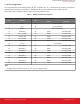

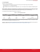

Table Of Contents
- 1. WFM200 Pinout
- 2. Device Configuration
- 3. Features Description
- 4. Power Supplies
- 5. Application Schematic Recommendations
- 6. Typical Application Schematics
- 7. Layout Recommendations
- 7.1 Generic RF Layout Considerations
- 7.2 GND and RF Pads Including the Diversity Port and External Antennas
- 7.3 Module Antenna
- 7.3.1 Small Board Size Recommendations for Good RF Performance
- 7.3.2 Extended X Dimension Recommendation for Good RF Performance
- 7.3.3 Y Dimension (65 to 80 mm) Recommendation for Good RF Performance
- 7.3.4 Y Dimension (80 mm or Larger) Recommendation for Good RF Performance
- 7.3.5 WFM200 Portion One Corner Bias with 3 mm Metal Keep-Outs
- 7.3.6 Recommended Antenna Loop Trace Capacitor Values
- 7.4 WFM200 Reference Evaluation Board
- 8. Recommendations for Certification
- 9. Package Outline
- 10. Integral Antenna Loop and Keep-Out Required Dimensions
- 11. Recommended PCB Land Pattern

4. Power Supplies
WFM200 has three power supply pins.
• VDD_PA supplies the Power amplifier. Recommended to have VDD_PA as the highest supply voltage of WFM200.
• VDD supplies the core, i.e., both RF and digital parts.
• VDD_IO supplies the pins and determines the voltage levels on pins, so this voltage should be compatible with WFM200 peripher-
als.
Bypass capacitors and filtering are included internally. If DC regulators are not placed sufficiently close to the supply pins to minimize
trace inductance and voltage drop, then additional external bypass caps (ceramics) may be required depending on application. Similar-
ly, it is recommended to use external bypass caps and series ferrite beads for supply pins fed by the same supply.
The requirements for these supplies are summarized in the table below:
Table 4.1. Power Supply Requirements
Pin # WFM200 Pin Name Min Voltage Max Voltage Typical Supply Current
10 VDD_PA 3.0 V 3.6 V ~100 mA
20 VDD 1.62 V VDD_PA ~40 mA
28 VDD_IO 1.62 V 3.6 V Upon SPI/SDIO frequency and load
Note: Although VDD_PA is variable, the maximum TX power can be achieved only when VDD_PA is set to 3.3 V minimum. For exam-
ple, the TX power may be slightly lower if VDD_PA is set to 3.0 V.
There are no specific pin requirements on supplies sequencing except that all supply voltages should be settled at the rising edge of the
RESETn pin, as shown in Figure 3.1 WFM200 Power Up and Host Interface Timing Parameters on page 7.
UG395: WFM200 Hardware Design User's Guide
Power Supplies
silabs.com | Building a more connected world. Preliminary Rev. 0.1 | 9