
Data Sheet
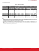


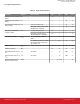

Table Of Contents
- wgm160p-datasheet-20190225 v2
- ug384-wgm160p-hardware-design-users-guide-20190225

4. Electrical Specifications
All electrical parameters in all tables are specified under the following conditions, unless stated otherwise:
• Typical values are based on T
AMB
= 25 °C; V
VBAT
= 3.3V; Center Frequency = 2,437 MHz.
• Radio performance numbers are measured in conducted mode, based on Silicon Laboratories reference designs using output pow-
er-specific external RF impedance-matching networks for interfacing to a 50 Ω antenna port. Conducted RF measurements include
additional output power reductions to guarantee WiFi and regulatory emissions compliance while connected to the specified anten-
nas which have non-ideal impedance loading.
Refer to Section 4.2 Operating Conditions for more details about operational supply and temperature limits.
4.1 Absolute Maximum Ratings
Stresses above those listed below may cause permanent damage to the device. This is a stress rating only and functional operation of
the devices at those or any other conditions above those indicated in the operation listings of this specification is not implied. Exposure
to maximum rating conditions for extended periods may affect device reliability. For more information on the available quality and relia-
bility data, see the Quality and Reliability Monitor Report at http://www.silabs.com/support/quality/pages/default.aspx.
Table 4.1. Absolute Maximum Ratings
Parameter Symbol Test Condition Min Typ Max Unit
Storage temperature T
STG
-40 — 105 °C
RF power level at RF1 and
RF2 ports
P
RFMAX
Max power that can be applied to
input of recommended matching
network connected to RF1 and
RF2 pins.
— — 10 dBm
Maximum supply voltage to
VBAT
VBAT
MAX
-0.3 — 3.6 V
DC voltage on I/O pins VG
MAX
5 V tolerant GPIO (PF0, PF1,
PF10, PF11)
1
2
-0.3 — Min of 5.25
and VBAT
+2
V
All other GPIO and PTA pins -0.3 — VBAT + 0.3 V
Current into any GPIO pin IO
MAX
— — 20 mA
Sum of current into all GPIO
pins
IO
ALLMAX
— — 150 mA
Range of load impedance at
RF1 and RF2 pins during TX
LOAD
TX
— — 10:1 VSWR
Note:
1. When a GPIO is used for analog functions via the APORT, the maximum voltage is VBAT.
2. To operate above the VBAT supply rail, over-voltage tolerance must be enabled according to the GPIO_Px_OVTDIS register.
Pins with over-voltage tolerance disabled have the same limits as all other GPIO (max = VBAT + 0.3 V).
WGM160P Wi-Fi
®
Module Data Sheet
Electrical Specifications
silabs.com | Building a more connected world. Preliminary Rev. 0.3 | 7