
User Manual


Description F-Pak
Features
Schematic Symbol
Applications
ESA / EFI
The Voltage Controlled Solidtron
TM
(VCS) features high peak
current capability and a low on-state voltage drop common to
SCR thyristors. Additionally if features extremely high turn-on
di/dt capability and virtually no turn-on delay jitter making it
ideally suited for a variety of capacitor discharge applications.
The 4-pin F-Pak SM package offers a rugged low inductance
interface and allows for installation using automated handling
equipment. The package consists of an epoxy filled 4 contact
FR4 substrate.
1400V Peak Off-State Voltage
3.0kA Repetitive Peak Anode Current
120kA/uSec dI/dt Capability
18nSec Turn-On Delay
Low Loss
MOS Gate Control
Anode (A)
VCSFF05N14A10
275 Great Valley Parkway
Malvern, PA 19355
Ph: 610-407-4700
fax: 610-407-3688
Solidtron
TM
N-MOS VCS, F-Pak
Data Sheet (Rev 6 - 06/17/11)
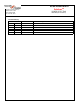
Limiting Characteristics and Ratings
SYMBOL VALUE UNITS
Peak Off-State Voltage
V
DRM
1400 V
Peak Reverse Voltage
V
RRM
-30 V
Off-State Rate of Change of Voltage Immunity (V
D
=1400V)
dv/dt
5000 V/uSec
Non-repetitive Peak Anode Current (Sinusoid Pulse Duration=250nSec)
I
ASM
4800 A
Repetitive Peak Anode Current (Sinusoid Pulse Duration=250nSec)
I
ASM
3000 A
Rate of Change of Current
dI/dt
120 kA/uSec
Continuous Gate-Cathode Voltage
V
GKS
+/-20 V
Peak Gate-Cathode Voltage
V
GKM
+/-25 V
Minimum Gate-Cathode Voltage Required for Guaranteed Off-State
V
GK(OFF-MIN)
0V
Maximum Junction Temperature
T
JM
125
o
C
Maximum Soldering Temperature (Installation) 260
o
C
Gate (G)
Cathode (K)
Gate Return (GR)