
User Manual


T
yp
ical Performance Curves
(
Continued
)
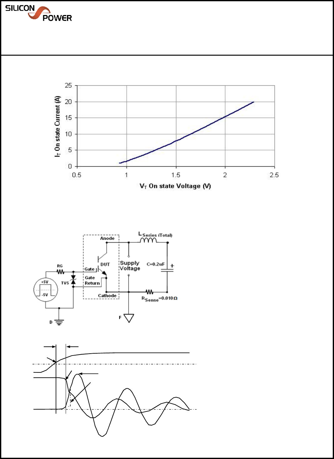
Figure 2 On state characteristics
Test Circuit and Waveforms
VCSFF05N14A10
Solidtron
TM
N-MOS VCS, F-Pak
Data Sheet (Rev 6 - 06/17/11)
275 Great Valley Parkway
Malvern, PA 19355
Ph: 610-407-4700
fax: 610-407-3688
L
i ltd i
Figure 3. 0.16uF Pulsed Discharge Circuit Schematic
Figure 4. 0.16uF Pulsed Discharge Circuit Waveforms
V
GK
V
AK
I
A
I
P
T
DELAY(ON)
0 Ref.
0 Ref.
90%
10%
dI/dt - 10% to 50% of I
P
The waveform shown is
representative of one produced
using a very low inductance circuit
(<10nH).
V
GK
is held positive until I
A
oscillations have ended ( I
A
=0).
•L
SERIES(TOTAL)
iscaculatedusing
1/(f2π)
2
Cwhere
f=frequencyofI
A
(SeeFigure4)
•R
SENSE
isacalibrated
CurrentViewingResistor(CVR)
•TVS‐ FairchildSMBJ9V0CA
•Gate drivercircuitgroundconnectedto
GR(GateReturn).Donotconnectgate
circuitgroundtocathodeexternaltothe
device.