
User's Manual


50 ohm PCB Design Guidelines
Antenna design and RF layout are critical in a wireless system that transmits and receives
electromagnetic radiation in free space. The Milli 5 module does not include an antenna
connector. The antenna (or unique antenna connector) must be connected to Milli 5 via a
transmission line implemented on the host PCB.
SSN recommends the use of a co-planer Waveguide to minimize space and board real
estate. The PCB trace should be kept as short as possible to minimize path loss.
IPC 6011 and IPC 6012 Class 2 or better PCB manufacturing practices must be followed to
ensure repeatable results.
The transmission line trace will be bounded on both sides by a ground reference plane. For
EMI considerations this ground plane should be extended and connected to other ground
layers, one of which is on the opposite side of the PCB. The opposite side ground plane
shall be contiguous under the trace and shall extend beyond the trace. These ground
planes should be stitched together using vias spaced 40-50 mils (2 mm) apart. Avoid
breaking up these ground planes by routing traces through them.
Avoid routing any other signal traces, especially high speed digital signals, near the
transmission line. Locate the transmission line trace away from power supply lines and
power supply regulatory circuitry.
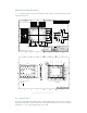
Key design parameters
The antenna trace must have a characteristic impedance of 50 Ω ± 5%. The recommended
dimensions and the Gerber layout for the antenna trace are provided on the following
pages. To calculate the key parameters requires calculating transmission line parameters.
Although there are many transmission line and trace impedance calculators found on-line,
they are not as thorough as specialized tools, and in simplifying the calculations, may omit
critical variables.
Silver Spring recommends the use of AppCAD Design Assistant. This software is available
as a free download from Avago Technologies:
http://www.avagotech.com/appcad
Additional support information on AppCAD can be found here:
http://www.hp.woodshot.com/
This reference design uses 1 oz copper. The base PCB material is ITEQ IT‑180A. Data sheet
is available here:
http://www.prototron.com/documents/materials/IT‑180A.pdf
which has an εᵣ specied as 4.4.