
User's Manual
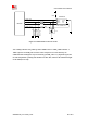
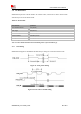
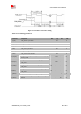
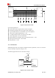
Table Of Contents
- RF Exposure Statement:
- General Notes
- Copyright
- Contents
- Table Index
- Figure Index
- Revision History
- 1Introduction
- 2Package Information
- 3Interface Application
- 3.1Power Supply
- Figure 5: VBAT voltage drop during burst emission
- 3.1.1Power Supply Design Guide
- Figure 6: Power supply application circuit
- Table 7: Recommended Zener diode list
- 3.1.2Recommended Power Supply Circuit
- Figure 7: Linear regulator reference circuit
- Figure 8: Switching mode power supply reference ci
- 3.1.3Voltage Monitor
- 3.2Power on/Power off/Reset Function
- 3.3UART Interface
- 3.4USB Interface
- 3.5USIM Interface
- 3.6PCM Interface
- 3.7SD Interface
- 3.8I2C Interface
- 3.9SDIO Interface
- 3.10SPI Interface
- 3.11Network status
- 3.12Flight Mode Control
- Switch
- 3.1Power Supply
- 4RF Specifications
- 5Electrical Specifications
- 6SMT Production Guide
- 7Packaging
- Appendix

SIM7600SA-H_User Manual_V1.00
2017-10-11
Smart Machine Smart Decision
Figure 23: Module to EXT codec timing
Table 15: PCM timing parameters
Parameter
Description
Min.
Typ.
Max.
Unit
T(sync)
PCM_SYNC cycle time
–
125
–
μs
T(synch)
PCM_SYNC high level time
–
488
–
ns
T(syncl)
PCM_SYNC low level time
–
124.5
–
μs
T(clk)
PCM_CLK cycle time
–
488
–
ns
T(clkh)
PCM_CLK high level time
–
244
–
ns
T(clkl)
PCM_CLK low level time
–
244
–
ns
T(susync)
PCM_SYNC setup time high before falling edge
of PCM_CLK
–
122
–
ns
T(hsync)
PCM_SYNC hold time after falling edge of
PCM_CLK
–
366
–
ns
T(sudin)
PCM_IN setup time before falling edge of
PCM_CLK
60
–
–
ns
T(hdin)
PCM_IN hold time after falling
edge
of
PCM_CLK
60
–
–
ns
T(pdout)
Delay from PCM_CLK rising to PCM_OUT valid
–
–
60
ns
T(zdout)
Delay from PCM_CLK falling to PCM_OUT
HIGH-Z
–
–
60
ns