
User's Manual
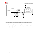
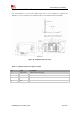
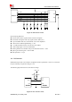
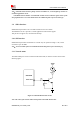
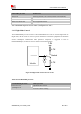
Table Of Contents
- RF Exposure Statement:
- General Notes
- Copyright
- Contents
- Table Index
- Figure Index
- Revision History
- 1Introduction
- 2Package Information
- 3Interface Application
- 3.1Power Supply
- Figure 5: VBAT voltage drop during burst emission
- 3.1.1Power Supply Design Guide
- Figure 6: Power supply application circuit
- Table 7: Recommended Zener diode list
- 3.1.2Recommended Power Supply Circuit
- Figure 7: Linear regulator reference circuit
- Figure 8: Switching mode power supply reference ci
- 3.1.3Voltage Monitor
- 3.2Power on/Power off/Reset Function
- 3.3UART Interface
- 3.4USB Interface
- 3.5USIM Interface
- 3.6PCM Interface
- 3.7SD Interface
- 3.8I2C Interface
- 3.9SDIO Interface
- 3.10SPI Interface
- 3.11Network status
- 3.12Flight Mode Control
- Switch
- 3.1Power Supply
- 4RF Specifications
- 5Electrical Specifications
- 6SMT Production Guide
- 7Packaging
- Appendix

SIM7600SA-H_User Manual_V1.00
2017-10-11
Smart Machine Smart Decision
Figure 25: SD reference circuit
SD card layout guide lines:
● Protect other sensitive signals/circuits from SD card signals.
● Protect SD card signals from noisy signals (clocks, SMPS, etc.).
● Up to 200 MHz clock rate, 50 Ω nominal, ±10% trace impedance
● CLK to DATA/CMD length matching < 1 mm
● 15–24 Ω termination resistor on clock lines near module
● Total routing length < 50 mm recommended
●
Routing distance from module clock pin to termination resistor < 5 mm
●
Spacing to all other signals = 2x line width
●
Bus capacitance < 15 pF
3.8 I2C Interface
SIM7600SA-H provides a I2C interface compatible with I2C specification, version 5.0, with clock
rate up to 400 kbps. Its operation voltage is 1.8V.
The following figure shows the I2C bus reference design.
VDD_1V8
2.2K
2.2K
SCL
SDA
SCL
SDA
GND
Module
GND
Module
Figure 26: I2C reference circuit
VCC
CMD
D3
GND
D2
D1
GND
D0
CLK
VDD_SD
SD Card
SD_CMD
SD_DATA3
SD_DATA2
Module
SD_DATA1
SD_DATA0
SD_CLK
TVS
TVS
TVS
TVS
TVS
TVS
100nF
4.7uF