
Hardware Design V1.00

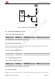


Table Of Contents
- Version History
- 1. Introduction
- 2. SIM2000S Overview
- 3. Package Information
- 4. Application Interface
- 4.1. Power Supply
- 4.2. Power on/down Scenarios
- 4.3. Power Saving Mode
- 4.4. Serial Port and Debug Interface
- 4.5. RI behaviors
- 4.6. Audio Interfaces
- 4.7. RUIM Card Interface
- 4.8. PCM Interface
- 4.9. Keypad Interface
- 4.10. I2C Bus
- 4.11. General Purpose Input/Output (GPIO)
- 4.12. ADC
- 4.13. PWM
- 4.14. Network Status Indication
- 4.15. NETLIGHT Multiplexing Function
- 4.16. Operating Status Indication
- 4.17. Antenna Interface
- 5. PCB Layout
- 6. Electrical, Reliability and Radio Characteristics
- 7. Manufacturing
- 8. Appendix

Smart Machine Smart Decision
5. PCB Layout
Usually, most electronic products with good performance are based on good PCB layout. A bad PCB layout will
lead to lots of issues, like RUIM card not being detected, etc. The final solution for these problems is to redo
PCB layout. Making good PCB layout at beginning will save development schedule and cost as well.
This section will give some guidelines on PCB layout, in order to eliminate interfere or noise by greatest degree,
and save product development period.
5.1 Pin Assignment
Before PCB layout, we should learn well about pin assignment in order to get reasonable layout with so many
external components. Following figure is the overview of pin assignment of the module.
Figure 39: Pin assignment
SIM2000S_Hardware_Design_V1.00 44 2014-02-27