
User's Manual

Skylab M&C Technology Co., Ltd
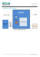
Module SKB369
SKB369-DA-001,A/1
5. Interfaces
5.1 Power Supply
Regulated power for the SKB369 is required. The input voltage Vcc range should be 1.7V to 3.6V.
Suitable decoupling must be provided by external decoupling circuitry (10uF and 0.1uF). It can reduce
the noise from power supply and increase power stability.
5.2 System Function Interfaces
5.2.1 GPIOs
The general purpose I/O is organized as one port with up to 19 I/Os enabling access and control of up
to 19 pins through one port. Each GPIO can be accessed individually with the following user
configurable features:
1、Input/output direction
2、Output drive strength
3、Internal pull-up and pull-down resistors
4、Wake-up from high or low level triggers on all pins
5、Trigger interrupt on all pins
6、All pins can be used by the PPI task/event system; the maximum number of pins that
can be interfaced through the PPI at the same time is limited by the number of GPIOTE channels
7、All pins can be individually configured to carry serial interface or quadrature demodulator signals
8、All pins can be configured as PWM signal.
9、There are 6 ADC/LPCOMP input in the 19 I/Os.
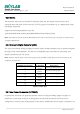
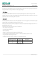
5.2.2 Two-wire Interface (I2C Compatible)
The two-wire interface can communicate with a bi-directional wired-AND bus with two lines (SCL,
SDA). The protocol makes it possible to interconnect up to 127 individually addressable devices. The
interface is capable of clock stretching, supporting data rates of 100 kbps ,250kbps and 400 kbps. The
module has 2 TWI ports and they properties like following table.
Bluetooth Module