
User's Manual


Skylab M&C Technology Co., Ltd
Module SKB369
SKB369-DA-001,A/1
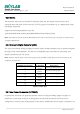
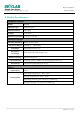
Instance
Master/Slave
TWI0
Master
TWI1
Master
Table5-1: TWI Pin Share Scheme
Note:I2C:Inter-Integrated Circuit
5.2.3 Flash Program I/Os
The module has two programmer pins, respectively SWDCLK pin and SWDIO pin. The two pin Serial
Wire Debug (SWD) interface provided as a part of the Debug Access Port (DAP) offers a flexible and
powerful mechanism for non-intrusive debugging of program code. Breakpoints and single stepping
are part of this support.
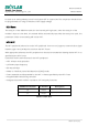
5.2.4 Serial Peripheral Interface
The SPI interfaces enable full duplex synchronous communication between devices. They support a
three-wire (SCK, MISO, MOSI) bi-directional bus with fast data transfers. The SPI Master can
communicate with multiple slaves using individual chip select signals for each of the slave devices
attached to a bus. Control of chip select signals is left to the application through use of GPIO signals.
SPI Master has double buffered I/O data. The SPI Slave includes EasyDMA for data transfer directly to
and from RAM allowing Slave data transfers to occur while the CPU is IDLE. The GPIOs are used for
each SPI interface line can be chosen from any GPIOs on the device and configed independently. This
enables great flexibility in device pinout and efficient use of printed circuit board space and signal
routing.
The SPI peripheral support SPI mode 0,1,2,and 3.The module have 3 SPI ports and theirs they
properties are as below:
Instance
Master/Slave
SPI0
Master
SPI1
Master
SPIS1
Slave
Table5-2: SPI Properties
Bluetooth Module