AN 12.12 LAN9118 Family Programmer Reference Guide 1 Introduction This application note describes how to successfully develop a network device driver for LAN9118 Family products. It covers device features, software design techniques, network operating system interfaces, and critical design points. It provides basic design guidelines for incorporating LAN9118 Family products into networked applications.
LAN9118 Family Programmer Reference Guide An octet or byte is a group of 8 bits, treated as a single unit, with a value of 0-255 unsigned, or 127 to +127 signed. A byte is generally the smallest unit of data that can be individually addressed. A word or short int is a group of 16 bits or two bytes,2 adjacent bytes, representing a 16-bit, single symbol or a numeric range from 0 – 65,535 unsigned, or +/- 32,767 as a signed value. WORD values are aligned on 2-byte memory boundaries.
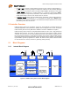
LAN9118 Family Programmer Reference Guide 2.1.2 System Level Block Diagram System Memory System Memory System Peripherals Microprocessor/ Microcontroller System Bus LAN9118 Family Member 25MHz XTAL Magnetics Ethernet LEDS/GPIO EEPROM (Optional) Figure 2.2 LAN9118 Family Device System-Level Block-Diagram 2.2 Common Product Family Features Single chip Ethernet controller Fully compliant with IEEE 802.3/802.
LAN9118 Family Programmer Reference Guide High-Performance host bus interface Simple SRAM-like interface Large, 16Kbyte FIFO memory with adjustable Tx/Rx allocation Memory Alignment Technology (MAT) supports interleaved transmit/receive/command/status access One configurable Host interrupt Burst read support Comprehensive power management features Numerous power management modes Wake on LAN “Packet-of-Interest” wakeup Wakeup indicator event signal Link Status Change Miscellaneous features Low pr
LAN9118 Family Programmer Reference Guide 3 Register Description Refer to the LAN9118 Family datasheets for complete descriptions of the Control and Status Registers (CSRs), as well as for descriptions of register and bit names, nomenclature and attributes used in this application note. Highlights are reproduced here for quick reference.
LAN9118 Family Programmer Reference Guide 3.1 Directly Addressable Registers These registers are also referred to as “Slave Registers”. Table 3.
LAN9118 Family Programmer Reference Guide 3.2 MAC Control and Status Registers The registers listed below are accessed indirectly through the MAC_CSR_CMD and MAC_CSR_DATA Registers. These registers are used in Section 5.1.2 and Section 5.5. . Table 3.
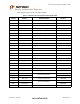
LAN9118 Family Programmer Reference Guide Table 3.3 LAN9118 Family PHY Control and Status Register PHY CONTROL AND STATUS REGISTERS INDEX (IN DECIMAL) 3.
LAN9118 Family Programmer Reference Guide Table 3.
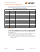
LAN9118 Family Programmer Reference Guide Table 3.5 Special Back-to-Back Cycles AFTER READING... PERFORM X READS OF BYTE_TEST BEFORE READING... RX Data FIFO 3 RX_FIFO_INF RX Status FIFO 3 RX_FIFO_INF TX Status FIFO 3 TX_FIFO_INF RX_DROP 4 RX_DROP 4 Programming Recommendations The fundamental operations of the driver are initialization, transmit packet processing, receive packet processing, and interrupt processing.
LAN9118 Family Programmer Reference Guide 4.4 Register Functionality in the LAN9118 Family Devices Table 4.1, "Independent Data Threads Register Usage" details the functions of the most important LAN9118 Family CSRs Table 4.
LAN9118 Family Programmer Reference Guide 4.5 An Example of Concurrency The need of maintaining the independence of the transmit and receive packet processing functions has already been mentioned.
LAN9118 Family Programmer Reference Guide The first example works because of the assumption that only one thread will ever write to the flag and signal the SwInt. The SwInt handler can use the flag to interpret the requested operation. This is known as a producer-consumer relationship. That is, it is safe for multiple threads to share a variable if only one thread is the writer, or producer of the variable, and all other threads are readers, or consumers of that variable. 4.
LAN9118 Family Programmer Reference Guide Table 4.2 Register Ownership Policy in the Simple Driver (continued) REGISTER NAME OWNERSHIP POLICY TX_FIFO_INF Read Only.
LAN9118 Family Programmer Reference Guide 5 Initialization 5.1 MAC Initialization The ID_REV register is a good starting point from which to begin initialization, in that it provides a known location in memory containing a known value; in the case of a LAN9118, revision B, the value is 0x1180001. Typical usage is twofold. One is as a probe point, while the other use is as a d i s c r i m i n a t o r o f t h e L A N 9 11 8 F a m i l y m e m b e r.
LAN9118 Family Programmer Reference Guide Besides the MAC address, no other values are automatically loaded to the controller from EEPROM in a reload cycle. 5.1.3.4 Saving the MAC Address to EEPROM A likely scenario during the manufacturing phase is to fix the MAC address of the host in the EEPROM after assembly. There may also be valid reasons where the driver would allow a user to change the MAC address after manufacture or startup.
LAN9118 Family Programmer Reference Guide has the bits corresponding with the interrupts to be enabled set to “1”. To disable specific interrupts, AND the contents with a bit-mask which has the bits corresponding to the interrupts to be disabled set to “0”. Write the modified value back to the register. Per Section 3.4 and Section 3.5, the INT_EN register requires a “settling” time before its effects are felt .
LAN9118 Family Programmer Reference Guide 5.5 Configuring Address Filtering Options Table 5.2, "Address Filtering Modes" shows the relations between the control flags which affect the address filter mode. Table 5.2 Address Filtering Modes MCPAS PRMS INVFILT HFILT HPFILT DESCRIPTION 0 0 0 0 0 MAC Address Perfect filtering only for all addresses.
LAN9118 Family Programmer Reference Guide 5.6 PHY Detection and Initialization Applications commonly delegate link set-up to the physical media device (PHY). At initialization, the driver can direct the PHY to determine the link parameters by auto-negotiating with its link partner (the link partner is the node on the other side of the Ethernet cable).
LAN9118 Family Programmer Reference Guide has completed, or else spurious operations could result. Setting of the CSR Address, R/nW and CSR busy bits can all be done with a single write command to the MAC_CSR_CMD Register. Table 5.
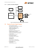
LAN9118 Family Programmer Reference Guide Host Processor Host Bus Interf ace Slave CSRs (Directly Addressable) Of f set 0xA4 MAC_CSR_CMD Register 0xA8 MAC_CSR_DataRegister MAC CSRs Index 0x6 MII_ACC_Register 0x7 MII_Data_Register ExternalMII (LAN9115 and LAN9117 InternalMII PHY Address = 00001b PHY Address /= 00001b PHY CSRs (Internal PHY) PHY RegisterIndex PHY CSRs (External PHY) 0 Basic Control Register 1 Basic Status Register 2 PHY ID Register1 3 PHY ID Register2 4 A/N Adv ertisem
LAN9118 Family Programmer Reference Guide Basic Control Register (index 0) and completes when the Auto-negotiate Complete bit (5) is set in the Basic Status Register (index 1). Auto-negotiate Complete status should be available within 1.5 seconds. Beyond this time, the driver can then probe for the reason of the failure, such as link down or remote fault, and additionally schedule a thread to revisit the PHY initialization periodically until a proper link has been established.
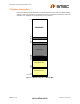
LAN9118 Family Programmer Reference Guide 1 Using SMI, Set Internal PHY and External PHY to a Stable State 8 Set EXT_PHY_SEL to Desired MII Port 2 Halt Transmitter 9 Set PHY_CLK_SEL to Desired MII Port 3 TX Stopped? 10 Clocks Running NO YES 4 5 NO YES Halt Receiver RX Stopped? 11 Enable RX 12 Enable TX 13 Complete NO YES 6 7 Set PHY_CLK_SEL to 10b Clocks Halted? NO YES Figure 5.2 The MII Switching Procedure 1.
LAN9118 Family Programmer Reference Guide 4. The PHY_CLK_SEL field must be set to 10b. This action will disable the MII clocks from the internal and external PHYs to the controller’s internal logic. 5. The host must wait a period of time not less than 5 cycles of the slowest operating PHY clock before executing the next step in this procedure.
LAN9118 Family Programmer Reference Guide Step Three: Keep reading the MAC_CSR_CMD Register until the CSR Busy Bit =0. Load the MII write command word (MII W/nR == 1) that is to be written to the MII ACC register into the MAC_CSR_Data register. The command word will write the contents of the MII DATA register to the PHY Advertisement register (0x4) (note that the lighter-shaded heading is expressed in MII ACC register terms).
LAN9118 Family Programmer Reference Guide MAC_CSR_CMD (ACCESSING MII_ACC REGISTER) CSR Busy R/nW 1 0 Reserved (29:8) CSR Address (7:0) 0x06 Steps Three - Seven: 3. Read the MAC_CSR_CMD Register until the CSR Busy Bit = 0. 4. Write the MAC_CSR_CMD as follows: Busy Bit = 1, R/nW = 1, CSR Address = 0x06. 5. Read the MAC_CSR_CMD Register until the CSR Busy Bit = 0 6. Read the MAC_CSR_Data Register.
LAN9118 Family Programmer Reference Guide 6 Transmit Packet Processing Transmitting packets is a straightforward process compared with receiving packets; in that the host can efficiently synchronize the entire transmit process with the application. In practice though, interrupts are still needed for synchronizing to the time-dependant embedded applications.
LAN9118 Family Programmer Reference Guide Last Segment is also a 1-bit field, marking the data transfer as the end of a single packet. To better understand the use of these last two fields, let’s discuss two popular operating systems that utilize different packet allocation schemes. Under Linux, system kernel buffers (skb’s) are used to hold packet data and almost always contain enough space for the largest possible packet size (1514 bytes) as an optimization of time-of-allocation.
LAN9118 Family Programmer Reference Guide 6.4 Packet Transfer Completion: Management Statistics Once a data packet has been transferred into the TX_Data_FIFO, most protocol stacks have no need for the sending thread to acknowledge the transfer result; the upper protocol layers are expected to deal with failures, such as a TCP layer re-transmit.
LAN9118 Family Programmer Reference Guide 6.5 Transmit Packet Examples Let’s take a look at Table 6.2, "Transmit Packet Example", which shows a 78-byte (0x4e) transmit packet used in the example, which begins at location 0xb4002013 in physical memory. In this case, it happens to be an IP packet to be sent from our MAC source address of 00:80:0f:71:55:71 to a destination MAC address of 00:0e:83:a0:de:ff. Table 6.
LAN9118 Family Programmer Reference Guide Table 6.4 Transmit Command Words TX_CMD_B Packet Tag 15 14 13 12 11 Packet Length 0x1234 0x4e Keep in mind that this example is running in a Little Endian environment. To begin the transfer sequence, write the two command words as DWORDs, followed by the packet data. Since the transfer is aligned on 4-byte boundaries, the data transfer start address must begin from 0xb4002010 and continue up to and including 0xb4002060. Table 6.
LAN9118 Family Programmer Reference Guide Data Transfers to the LAN911x Data Passed on to the TX Data FIFO 31 0 TX Command A Word TX Command B Word TX Command B Word 3-byte Data Start Offset TX Command ‘A’ Buffer End Alignment = 1 Data Start Offset = 3 First Segment = 1 Last Segment = 0 Buffer Size = 29 29-byte Payload Data TX Command ‘B’ Packet Length = 78 78-byte Payload Data 31 0 TX Command A Word TX Command ‘A’ Buffer End Alignment = 1 Data Start Offset = 3 First Segment = 0 Last Segment =
LAN9118 Family Programmer Reference Guide 6.5.1 Transmit Command Words for Figure 6.1, "Multiple (3) Buffer Data Single Packet Transfer Sequence" Table 6.6 TX_CMD_A for Segment 1 3 1 3 0 2 9 2 8 2 7 2 6 BUFFER END ALIGNME NT 2 3 2 2 2 1 0x0 DATA START OFFSET 1 5 1 4 LAST SEGME NT FIRST SEGMENT 0x3 1 1 1 BUFFER SIZE 0 0x1d Table 6.7 TX_CMD_B for Segment 1 PACKET TAG 15 14 13 12 PACKET LENGTH 11 0x5678 0x4e Table 6.
LAN9118 Family Programmer Reference Guide Table 6.
LAN9118 Family Programmer Reference Guide Hard Transmit Packet Accumulated TX stats to process? Y Schedule NOS thread to evaluate TX Status for each packet sent, accumulate common driver statistics and clear TX Status FIFO N TDFA Interrupt: TDFREE threshold reached Transfer TX Cmd Words, Data Memory Buffer to TX Data FIFO Interrupt Service Routine Free up NOS Data Memory Buffer Disable TDFA_INT_EN interrupt on FIFO_INT:TX Data Available Level exceeding marker Can the FIFO accept the next packet? (
LAN9118 Family Programmer Reference Guide 7 Receive Packet Processing A receive process must signal the host that there are incoming packets to be read in, it must identify the validity and length of each individual packet, copy the packet data from device to memory, hand off the packet data memory to the protocol stack, maintain count statistics, and continue the application when there are no more incoming packets.
LAN9118 Family Programmer Reference Guide Rx Process Packets Read Rx Status Rx Status errors? RSFL Interrupt: FIFO_INT:RX Status Level threshold crossed Y N Interrupt Service Routine Multicast match? N Y 802.
LAN9118 Family Programmer Reference Guide 7.1 Receive Data Transfer Given that the device makes all data transfers in DWORD pieces, the driver can easily align the receiving data memory address to a DWORD boundary. Recall too, that the data transfer length must also be rounded up when considering overall data buffer length (i.e., a 109-byte packet should be treated as a 4*28 or 112 byte transfer). The RX Data Offset field gives the driver control over packet alignment Table 7.
LAN9118 Family Programmer Reference Guide : Table 7.3 RX End Alignment ALIGNMENT REQUIREMENT VALUE (31:30) 4-word alignment 0x0 16-word alignment 0x1 32-word alignment 0x2 (undefined, illegal) 0x3 Enabling a receive transfer requires setting up the RX_CFG register, shown in Table 7.4, "Receiver Configuration Word" below.
LAN9118 Family Programmer Reference Guide RX_DATA_FIFO must be read an appropriate number of DWORDS to purge the miniscule packet. This should only happen if the MAC_CR is configured to PASSBAD packets ( == ‘1’). 7.3 Flow Control Function The flow control function monitors space available in the RX Data FIFO.
LAN9118 Family Programmer Reference Guide 8 Instrumentation and Debug This chapter is based upon the experience gained from the development of the simple Linux Driver for the LAN9118 family. It assumes that the driver will have a rich feature set in its run-time environment to draw upon for debugging. While not every operating system offers the functionality of a Linux, the concepts remain useful and are offered to the driver developer as tips.
LAN9118 Family Programmer Reference Guide 8.1.3 SMSC_ASSERT(condition) SMSC_ASSERT points are enabled when USE_ASSERT is defined during compile time. It has no run time dependency on debug mode. This macro is used to test assumptions made when coding. It is useful to ensure consistency of logic through out the driver. It is only intended to be used in situations where a failure of the condition is fatal.
LAN9118 Family Programmer Reference Guide Figure 8.1 Oscilloscope/Logic Analyzer Display GPIOs can also be used with a scope for instrumentation. Most scopes provide a way to measure the time between events. In the trace above, the scope could be used to measure the time between the rising and falling edges of GP_1, revealing the length of time it takes to read a packet out of the Rx data FIFO with high accuracy. Measurements of the low time could be used to calculate the percentage of bus usage.
LAN9118 Family Programmer Reference Guide Some other useful error interrupts to be aware of include: 8.5 TXSO TDFO TSFF – TX status FIFO full RSFF – RX status FIFO full Integrating the Driver: Early Testing When the driver development has come to the point where it is being integrated into the protocol stack, a basic integration test which is useful for shaking out the data flows is to send the host a stream of ICMP ping request packets, while looking for the ping responses.
LAN9118 Family Programmer Reference Guide 80 ARKAY DRIVE, HAUPPAUGE, NY 11788 (631) 435-6000, FAX (631) 273-3123 Copyright © 2009 SMSC or its subsidiaries. All rights reserved. Circuit diagrams and other information relating to SMSC products are included as a means of illustrating typical applications. Consequently, complete information sufficient for construction purposes is not necessarily given.