LAN9500/LAN9500i Hi-Speed USB 2.0 to 10/100 Ethernet Controller PRODUCT FEATURES Datasheet Highlights — — — — — — Single Chip Hi-Speed USB 2.0 to 10/100 Ethernet Controller Integrated 10/100 Ethernet MAC with Full-Duplex Support Integrated 10/100 Ethernet PHY with HP Auto-MDIX support Integrated USB 2.0 Hi-Speed Device Controller Integrated USB 2.
Hi-Speed USB 2.0 to 10/100 Ethernet Controller Datasheet ORDER NUMBER(S): LAN9500-ABZJ FOR 56-PIN, QFN LEAD-FREE ROHS COMPLIANT PACKAGE (0 TO +70°C TEMP RANGE) LAN9500i-ABZJ FOR 56-PIN, QFN LEAD-FREE ROHS COMPLIANT PACKAGE (-40 TO +85°C TEMP RANGE) 80 ARKAY DRIVE, HAUPPAUGE, NY 11788 (631) 435-6000, FAX (631) 273-3123 Copyright © 2008 SMSC or its subsidiaries. All rights reserved. Circuit diagrams and other information relating to SMSC products are included as a means of illustrating typical applications.
Hi-Speed USB 2.0 to 10/100 Ethernet Controller Datasheet Table of Contents Chapter 1 Introduction . . . . . . . . . . . . . . . . . . . . . . . . . . . . . . . . . . . . . . . . . . . . . . . . . . . . . . . 6 1.1 Block Diagram . . . . . . . . . . . . . . . . . . . . . . . . . . . . . . . . . . . . . . . . . . . . . . . . . . . . . . . . . . . . . . . . . 1.1.1 Overview . . . . . . . . . . . . . . . . . . . . . . . . . . . . . . . . . . . . . . . . . . . . . . . . . . . . . . . . . . . . . . 1.1.2 USB . .
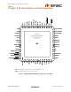
Hi-Speed USB 2.0 to 10/100 Ethernet Controller Datasheet List of Figures Figure 1.1 Figure 2.1 Figure 4.1 Figure 4.2 Figure 4.3 Figure 4.4 Figure 4.1 Figure 4.2 Figure 5.1 Figure 5.2 LAN9500/LAN9500i System Diagram . . . . . . . . . . . . . . . . . . . . . . . . . . . . . . . . . . . . . . . . . . . 6 LAN9500/LAN9500i 56-QFN Pin Assignments (TOP VIEW). . . . . . . . . . . . . . . . . . . . . . . . . . 9 Output Equivalent Test Load . . . . . . . . . . . . . . . . . . . . . . . . . . . . . . . . . . . . . .
Hi-Speed USB 2.0 to 10/100 Ethernet Controller Datasheet List Of Tables Table 2.1 MII Interface Pins. . . . . . . . . . . . . . . . . . . . . . . . . . . . . . . . . . . . . . . . . . . . . . . . . . . . . . . . . . . Table 2.2 EEPROM Pins . . . . . . . . . . . . . . . . . . . . . . . . . . . . . . . . . . . . . . . . . . . . . . . . . . . . . . . . . . . . . Table 2.3 JTAG Pins . . . . . . . . . . . . . . . . . . . . . . . . . . . . . . . . . . . . . . . . . . . . . . . . . . . . . . . . . . . . . . . .
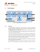
Hi-Speed USB 2.0 to 10/100 Ethernet Controller Datasheet Chapter 1 Introduction 1.1 USB Block Diagram USB PHY USB 2.0 Device Controller FIFO Controller 10/100 Ethernet MAC Ethernet PHY Ethernet MII: To optional external PHY JTAG TAP Controller SRAM EEPROM Controller EEPROM LAN9500/LAN9500i Figure 1.1 LAN9500/LAN9500i System Diagram 1.1.1 Overview The LAN9500/LAN9500i is a high performance Hi-Speed USB 2.0 to 10/100 Ethernet controller.
Hi-Speed USB 2.0 to 10/100 Ethernet Controller Datasheet 1.1.2 USB The USB portion of the LAN9500/LAN9500i integrates a Hi-Speed USB 2.0 device controller and USB PHY. The USB device controller contains a USB low-level protocol interpreter which implements the USB bus protocol, packet generation/extraction, PID/Device ID parsing, and CRC coding/decoding, with autonomous error handling. The USB device controller is capable of operating in USB 2.
Hi-Speed USB 2.0 to 10/100 Ethernet Controller Datasheet 1.1.6 EEPROM Controller The LAN9500/LAN9500i contains an EEPROM controller for connection to an external EEPROM. This allows for the automatic loading of static configuration data upon power-on reset, pin reset, or software reset. The EEPROM can be configured to load USB descriptors, USB device configuration, and MAC address. 1.1.7 General Purpose I/O When configured for internal PHY mode, up to eleven GPIOs are supported.
Hi-Speed USB 2.
Hi-Speed USB 2.0 to 10/100 Ethernet Controller Datasheet Table 2.1 MII Interface Pins BUFFER TYPE NUM PINS NAME SYMBOL Receive Error (External PHY Mode) RXER 1 IS (PD) Receive Error: In external PHY mode, the signal on this pin is input from the external PHY and indicates a receive error in the packet. In internal PHY mode, this pin is not used.
Hi-Speed USB 2.0 to 10/100 Ethernet Controller Datasheet Table 2.1 MII Interface Pins (continued) NUM PINS 1 BUFFER TYPE NAME SYMBOL Transmit Data 3 (External PHY Mode) TXD3 O8 (PU) General Purpose I/O 7 (Internal PHY Mode Only) GPIO7 IS/O8/ OD8 (PU) EEPROM Size Configuration Strap EEP_SIZE IS (PU) DESCRIPTION Transmit Data 3: In external PHY mode, this pin functions as the transmit data 3 output to the external PHY.
Hi-Speed USB 2.0 to 10/100 Ethernet Controller Datasheet Table 2.1 MII Interface Pins (continued) NUM PINS 1 BUFFER TYPE NAME SYMBOL Transmit Data 1 (External PHY Mode) TXD1 O8 (PD) General Purpose I/O 5 (Internal PHY Mode Only) GPIO5 IS/O8/ OD8 (PU) Remote Wakeup Configuration Strap RMT_WKP IS (PD) DESCRIPTION Transmit Data 1: In external PHY mode, this pin functions as the transmit data 1 output to the external PHY.
Hi-Speed USB 2.0 to 10/100 Ethernet Controller Datasheet Table 2.2 EEPROM Pins BUFFER TYPE NUM PINS NAME SYMBOL 1 EEPROM Data In EEDI IS (PD) EEPROM Data In: This pin is driven by the EEDO output of the external EEPROM. EEPROM Data Out EEDO O8 (PU) EEPROM Data Out: This pin drives the EEDI input of the external EEPROM. Auto-MDIX Enable Configuration Strap AUTOMDIX_EN IS (PU) Auto-MDIX Enable Configuration Strap: Determines the default Auto-MDIX setting.
Hi-Speed USB 2.0 to 10/100 Ethernet Controller Datasheet Table 2.3 JTAG Pins (continued) NUM PINS BUFFER TYPE NAME SYMBOL DESCRIPTION JTAG Test Clock (Internal PHY Mode) TCK IS (PU) JTAG Test Clock: In internal PHY mode, this pin functions as the JTAG test clock. The maximum operating frequency of this clock is 25MHz. Receive Data 1 (External PHY Mode) RXD1 IS (PD) Receive Data 1: In external PHY mode, this signal functions as the receive data 1 input from the external PHY.
Hi-Speed USB 2.0 to 10/100 Ethernet Controller Datasheet Table 2.4 Miscellaneous Pins (continued) NUM PINS BUFFER TYPE NAME SYMBOL Ethernet Link Activity Indicator LED nLNKA_LED OD12 (PU) General Purpose I/O 9 GPIO9 IS/O12/ OD12 (PU) Ethernet Speed Indicator LED nSPD_LED OD12 (PU) General Purpose I/O 10 GPIO10 IS/O12/ OD12 (PU) Detect Upstream VBUS Power VBUS_DET IS_5V (PD) Test 1 TEST1 - Test 1: This pin must always be connected to VDD33IO for proper operation.
Hi-Speed USB 2.0 to 10/100 Ethernet Controller Datasheet Table 2.5 USB Pins NUM PINS 1 1 1 1 NAME SYMBOL BUFFER TYPE USB DMINUS USBDM AIO USB DPLUS USBDP External USB Bias Resistor. USBRBIAS AI External USB Bias Resistor: Used for setting HS transmit current level and on-chip termination impedance. Connect to an external 12K 1.0% resistor to ground. USB PLL +1.8V Supply VDD18USBPLL P USB PLL +1.8V Supply: This pin must be connected to VDD18CORE for proper operation.
Hi-Speed USB 2.0 to 10/100 Ethernet Controller Datasheet Table 2.6 Ethernet PHY Pins (continued) NUM PINS NAME SYMBOL BUFFER TYPE PHY Interrupt (Internal PHY Mode) nPHY_INT O8 DESCRIPTION PHY Interrupt (Active-Low): In internal PHY mode, this signal can be configured to output the internal PHY interrupt signal. Note: 1 The internal PHY interrupt signal is active-high.
Hi-Speed USB 2.0 to 10/100 Ethernet Controller Datasheet Table 2.
Hi-Speed USB 2.0 to 10/100 Ethernet Controller Datasheet 2.1 Buffer Types Table 2.10 Buffer Types BUFFER TYPE IS IS_5V O8 DESCRIPTION Schmitt-triggered Input 5V Tolerant Schmitt-triggered Input Output with 8mA sink and 8mA source OD8 Open-drain output with 8mA sink O12 Output with 12mA sink and 12mA source OD12 PU Open-drain output with 12mA sink 50uA (typical) internal pull-up. Unless otherwise noted in the pin description, internal pullups are always enabled.
Hi-Speed USB 2.0 to 10/100 Ethernet Controller Datasheet Chapter 3 EEPROM Controller (EPC) LAN9500/LAN9500i may use an external EEPROM to store the default values for the USB descriptors and the MAC address. The EEPROM controller supports most “93C46” type EEPROMs. The EEP_SIZE strap selects the size of the EEPROM attached to LAN9500/LAN9500i. When this strap is set to “0”, a 128 byte EEPROM is attached and a total of seven address bits are used.
Hi-Speed USB 2.0 to 10/100 Ethernet Controller Datasheet Table 3.
Hi-Speed USB 2.0 to 10/100 Ethernet Controller Datasheet 3.2 EEPROM Defaults The signature value of 0xA5 is stored at address 0. A different signature value indicates to the EEPROM controller that no EEPROM or an un-programmed EEPROM is attached to LAN9500/LAN9500i. In this case, the hardware default values are used, as shown in Table 3.3. Table 3.
Hi-Speed USB 2.0 to 10/100 Ethernet Controller Datasheet 3.4 An Example of EEPROM Format Interpretation Table 3.4 and Table 3.5 provide an example of how the contents of a EEPROM are formatted. Table 3.4 is a dump of the EEPROM memory (256-byte EEPROM), while Table 3.5 illustrates, byte by byte, how the EEPROM is formatted. Table 3.
Hi-Speed USB 2.0 to 10/100 Ethernet Controller Datasheet Table 3.5 EEPROM Example - 256 Byte EEPROM EEPROM ADDRESS EEPROM CONTENTS (HEX) 00h A5 01h - 06h 12 34 56 78 9A BC 07h 01 Full-Speed Polling Interval for Interrupt Endpoint (1ms) 08h 04 Hi-Speed Polling Interval for Interrupt Endpoint (4ms) 09h 04 Configuration Flags - LAN9500/LAN9500i is bus powered and supports remote wakeup.
Hi-Speed USB 2.0 to 10/100 Ethernet Controller Datasheet Table 3.
Hi-Speed USB 2.0 to 10/100 Ethernet Controller Datasheet Table 3.
Hi-Speed USB 2.0 to 10/100 Ethernet Controller Datasheet Table 3.
Hi-Speed USB 2.0 to 10/100 Ethernet Controller Datasheet Chapter 4 Operational Characteristics 4.1 Absolute Maximum Ratings* Supply Voltage (VDD33IO, VDD33A) (Note 4.1) . . . . . . . . . . . . . . . . . . . . . . . . . . . . . . . . . 0V to +3.6V Positive voltage on signal pins, with respect to ground (Note 4.2) . . . . . . . . . . . . . . . . . . . . . . . . . . +6V Negative voltage on signal pins, with respect to ground (Note 4.3) . . . . . . . . . . . . . . . . . . . . . . . . -0.
Hi-Speed USB 2.0 to 10/100 Ethernet Controller Datasheet 4.3 Power Consumption This section details the power consumption of LAN9500/LAN9500i as measured during various modes of operation. Power consumption values are provided for both the device-only, and for the device plus Ethernet components. Power dissipation is determined by temperature, supply voltage, and external source/sink requirements. 4.3.1 SUSPEND0 Table 4.1 SUSPEND0 - Supply and Current @3.
Hi-Speed USB 2.0 to 10/100 Ethernet Controller Datasheet 4.3.4 Operational Power Consumption Table 4.4 Operational Power Consumption - Supply and Current @3.3V PARAMETER MIN TYPICAL MAX UNIT 100BASE-TX Full Duplex (USB High-Speed) Supply current (VDD33IO, VDD33A) 137.3 mA Power Dissipation (Device Only) 453.0 mW Power Dissipation (Device and Ethernet components) 591.2 mW Supply current (VDD33IO, VDD33A) 99.2 mA Power Dissipation (Device Only) 327.
Hi-Speed USB 2.0 to 10/100 Ethernet Controller Datasheet 4.4 DC Specifications Table 4.6 I/O Buffer Characteristics PARAMETER SYMBOL MIN Low Input Level VILI -0.3 High Input Level VIHI Negative-Going Threshold VILT 1.01 Positive-Going Threshold VIHT SchmittTrigger Hysteresis (VIHT - VILT) TYP MAX UNITS NOTES IS Type Input Buffer V 3.6 V 1.18 1.35 V Schmitt trigger 1.39 1.6 1.
Hi-Speed USB 2.0 to 10/100 Ethernet Controller Datasheet Note 4.6 This is the total 5.5V input leakage for the entire device. Note 4.7 XI can optionally be driven from a 25MHz single-ended clock oscillator. Table 4.7 100BASE-TX Transceiver Characteristics PARAMETER SYMBOL MIN TYP MAX UNITS NOTES Peak Differential Output Voltage High VPPH 950 - 1050 mVpk Note 4.8 Peak Differential Output Voltage Low VPPL -950 - -1050 mVpk Note 4.
Hi-Speed USB 2.0 to 10/100 Ethernet Controller Datasheet 4.5 AC Specifications This section details the various AC timing specifications of the LAN9500/LAN9500i. Note: The MII timing adheres to the IEEE 802.3 specification. Refer to the IEEE 802.3 specification for detailed MII timing information. Note: The USBDP and USBDM pin timing adheres to the USB 2.0 specification. Refer to the Universal Serial Bus Revision 2.0 specification for detailed USB timing information. 4.5.
Hi-Speed USB 2.0 to 10/100 Ethernet Controller Datasheet 4.5.2 Power-On Configuration Strap Valid Timing Figure 4.2 illustrates the configuration strap valid timing requirement in relation to power-on. In order for valid configuration strap values to be read at power-on, the following timing requirements must be met. VDD33IO 2.0V tcfg Configuration Straps Figure 4.2 Power-On Configuration Strap Valid Timing Table 4.
Hi-Speed USB 2.0 to 10/100 Ethernet Controller Datasheet 4.5.3 Reset and Configuration Strap Timing Figure 4.3 illustrates the nRESET pin timing requirements and its relation to the configuration strap pins and output drive. Assertion of nRESET is not a requirement. However, if used, it must be asserted for the minimum period specified. trstia nRESET tcss tcsh Configuration Strap Pins todad Output Drive Figure 4.3 nRESET Reset Pin Timing Table 4.
Hi-Speed USB 2.0 to 10/100 Ethernet Controller Datasheet 4.5.4 EEPROM Timing The following specifies the EEPROM timing requirements for LAN9500/LAN9500i: tcsl EECS tcshckh tckcyc tckh tckl tcklcsl EECLK tckldis tdvckh tckhdis EEDO tdsckh tdhckh EEDI tdhcsl tcshdv EEDI (VERIFY) Figure 4.4 EEPROM Timing Table 4.
Hi-Speed USB 2.0 to 10/100 Ethernet Controller Datasheet 4.5.5 Turbo MII Interface Timing The external MII supports Turbo MII and the interface timing is as follows. toutdly ttxhold TXCLK TXD[3:0] TXEN CRS Figure 4.1 Turbo MII Output Timing Table 4.12 Turbo MII Output Timing Values SYMBOL DESCRIPTION MIN toutdly Clock to output delay for TXD and TXEN ttxhold TXD and TXEN hold time after TXCLK MAX UNITS NOTES 12.5 ns Note 4.12 Note 4.13 ns Note 4.13 1.5 Note 4.
Hi-Speed USB 2.0 to 10/100 Ethernet Controller Datasheet Table 4.13 Turbo MII Interface Timing Values SYMBOL DESCRIPTION MIN trxsetup RXD and RXDV setup time prior to rising edge of RXCLK trxhold RXD and RXDV hold time after the rising edge of RXCLK MAX UNITS NOTES 5.5 ns Note 4.14 0 ns Note 4.14 Note 4.14 These values satisfy the 10-ns setup and hold time requirements that are necessary for the Turbo MII specification. Revision 1.
Hi-Speed USB 2.0 to 10/100 Ethernet Controller Datasheet 4.6 Clock Circuit LAN9500/LAN9500i can accept either a 25MHz crystal (preferred) or a 25MHz single-ended clock oscillator (+/- 50ppm) input. If the single-ended clock oscillator method is implemented, XO should be left unconnected and XI should be driven with a nominal 0-3.3V clock signal. The input clock duty cycle is 40% minimum, 50% typical and 60% maximum.
Hi-Speed USB 2.0 to 10/100 Ethernet Controller Datasheet Chapter 5 Package Outline Figure 5.1 LAN9500/LAN9500i 56-QFN Package Table 5.1 LAN9500/LAN9500i 56-QFN Dimensions MIN NOMINAL MAX REMARKS A 0.70 - 1.00 Overall Package Height A1 0.00 0.02 0.05 Standoff A2 - - 0.90 Mold Cap Thickness D/E 7.85 8.00 8.15 X/Y Body Size D1/E1 7.55 - 7.95 X/Y Mold Cap Size D2/E2 5.75 5.90 6.05 X/Y Exposed Pad Size L 0.30 - 0.50 Terminal Length b 0.18 0.25 0.
Hi-Speed USB 2.0 to 10/100 Ethernet Controller Datasheet Figure 5.2 LAN9500/LAN9500i 56-QFN Recommended PCB Land Pattern SMSC LAN9500/LAN9500i 41 DATASHEET Revision 1.
Hi-Speed USB 2.0 to 10/100 Ethernet Controller Datasheet Chapter 6 Revision History Table 6.1 Customer Revision History REVISION LEVEL AND DATE Rev. 1.6 (09-09-08) SECTION/FIGURE/ENTRY CORRECTION All Fixed various typos Table 3.4, “Dump of EEPROM Memory,” on page 23 Fixed typos in example Table 3.5, “EEPROM Example 256 Byte EEPROM,” on page 24 Fixed typos in example Table 2.
Hi-Speed USB 2.0 to 10/100 Ethernet Controller Datasheet Table 6.1 Customer Revision History (continued) REVISION LEVEL AND DATE SMSC LAN9500/LAN9500i SECTION/FIGURE/ENTRY CORRECTION Table 2.4, “Miscellaneous Pins,” on page 14 Added new TEST3 entry, which must always be grounded. Modified buffer types for TEST1 and TEST2 entries to indicate “-” as buffer type. Buffer type now hidden. TEST3 corresponds to hidden TESTMODE pin. Figure 2.