
- Standard Microsystems USB 2.0 Multi-Slot Flash Media ControllerDatasheet


Ultra Fast USB 2.0 Multi-Slot Flash Media Controller
Datasheet
Revision 1.1 (05-29-08) 12 SMSC USB2250/50i/51/51i
DATASHEET
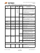
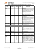
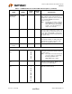
CF Data 7-0 /
GPIO
CF_D[7:0] /
GPIO[23:16]
69
67
63
61
59
88
86
85
I/O12PD CF_D[7:0]: The bi-directional data signals
CF_D7 - CF_D0 in True IDE mode data
transfer. In True IDE Mode, all of the task file
register operations occur on the CF_D[7:0],
while data transfer occurs on CF_D[15:0].
The bi-directional data signal has an internal
weak pull-down resistor.
I/O12 GPIO[23:16]: These Pins are GPIOs if the
CF_INTF_EN bit of the CFC_ATA_MODE
CTL is disabled and the EXTENDED_GPIO
bit set in UTIL_CONFIG1 is enabled.
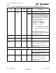
IO Ready CF_IORDY 80 IPU This pin is the active high input signal for
IORDY.
This pin has an internal weak pull-up resistor
that can be controlled by:
CF_INTF_EN bit of CFC_ATA_MODE CTL.
CF Card
Detection1
GPIO13
(CF_nCD)
58 I/O12 This is a GPIO designated as the Compact
Flash card detection pin.
CF Hardware
Reset
CF_nRESET 79 O12 This pin is an active low hardware reset
signal to the CF device.
CF IO Read CF_nIOR 72 O12 This pin is an active low read strobe signal
for the CF device.
CF IO Write
Strobe
CF_nIOW 73 O12 This pin is an active low write strobe signal
for the CF device.
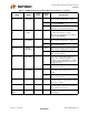
CF DMA request CF_DMARQ /
RXD / GPIO2
117 I CF_DMARQ: This pin is the DMA request
from the device to the CF controller.
RXD: The signal can be used as input to the
RXD of UART in the device when the
TXD_RXD_SEL bit in UTIL_CONFIG1
register is cleared to "0".
I/O12 GPIO: This pin may be used either as input,
edge sensitive interrupt input, or output.
CF DMA
acknowledge
CF_DMACK/
TXD / GPIO
119 O12 CF_nDMACK: This pin is an active low dma
acknowledge signal for the CF device.
TXD: GPIO7 can be used as an output TXD
of UART in the device, when the GPIO2/TXD
bit in UTL_CONFIG register is set to "1".
I/O12 GPIO: This pin may be used either as input,
edge sensitive interrupt input, or output.
SMART MEDIA INTERFACE
SM Write Protect SM_nWP 47 O12PD This pin is an active low write protect signal
for the SM device.
This pin has a weak pull-down resistor that
is permanently enabled.
Table 5.1 USB2250/50i/51/51i 128-Pin VTQFP Pin Descriptions (continued)
NAME SYMBOL
128-PIN
VTQFP
BUFFER
TYPE DESCRIPTION