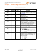
USB3290 Small Footprint Hi-Speed USB 2.0 Device PHY with UTMI Interface PRODUCT FEATURES Datasheet Available in a 40 ball lead-free RoHS compliant (4 x 4 x 0.9mm) VFBGA package Interface compliant with the UTMI specification (60MHz, 8-bit bidirectional interface) Only one required power supply (+3.3V) Supports 480Mbps Hi-Speed (HS) and 12Mbps Full Speed (FS) serial data transmission rates Integrated 45Ω and 1.
Small Footprint Hi-Speed USB 2.0 Device PHY with UTMI Interface Datasheet ORDER NUMBER(S): USB3290-FH FOR 40 BALL, VFBGA LEAD-FREE ROHS COMPLIANT PACKAGE USB3290-FH-TR FOR 40 BALL, VFBGA LEAD-FREE ROHS COMPLIANT PACKAGE (TAPE AND REEL) Reel Size is 4000 pieces. 80 ARKAY DRIVE, HAUPPAUGE, NY 11788 (631) 435-6000, FAX (631) 273-3123 Copyright © 2007 SMSC or its subsidiaries. All rights reserved.
Small Footprint Hi-Speed USB 2.0 Device PHY with UTMI Interface Datasheet Table of Contents Chapter 1 General Description . . . . . . . . . . . . . . . . . . . . . . . . . . . . . . . . . . . . . . . . . . . . . . . . . 6 1.1 Product Description . . . . . . . . . . . . . . . . . . . . . . . . . . . . . . . . . . . . . . . . . . . . . . . . . . . . . . . . . . . . . 6 Chapter 2 Functional Block Diagram . . . . . . . . . . . . . . . . . . . . . . . . . . . . . . . . . . . . . . . . . . .
Small Footprint Hi-Speed USB 2.0 Device PHY with UTMI Interface Datasheet List of Figures Figure 2.1 Figure 3.1 Figure 6.1 Figure 6.2 Figure 6.3 Figure 6.4 Figure 6.5 Figure 7.1 Figure 7.2 Figure 7.3 Figure 7.4 Figure 7.5 Figure 7.6 Figure 7.7 Figure 8.1 Figure 8.2 Figure 8.3 Figure 8.4 Figure 8.5 Figure 8.6 Figure 8.7 Figure 8.8 Figure 8.9 Figure 8.10 Figure 9.1 USB3290 Block Diagram . . . . . . . . . . . . . . . . . . . . . . . . . . . . . . . . . . . . . . . . . . . . . . . . . . . . .
Small Footprint Hi-Speed USB 2.0 Device PHY with UTMI Interface Datasheet List of Tables Table 4.1 System Interface Signals . . . . . . . . . . . . . . . . . . . . . . . . . . . . . . . . . . . . . . . . . . . . . . . . . . . . . . 9 Table 4.2 Data Interface Signals . . . . . . . . . . . . . . . . . . . . . . . . . . . . . . . . . . . . . . . . . . . . . . . . . . . . . . . 10 Table 4.3 USB I/O Signals. . . . . . . . . . . . . . . . . . . . . . . . . . . . . . . . . . . . . . . . . . . . . . . . . . . . .
Small Footprint Hi-Speed USB 2.0 Device PHY with UTMI Interface Datasheet Chapter 1 General Description The USB3290 provides the Physical Layer (PHY) interface to a USB 2.0 Device Controller. The IC is available in a 40 ball lead-free RoHS compliant VFBGA package. The small footprint package makes the USB3290 ideal for portable consumer electronics applications. 1.1 Product Description The USB3290 is an industrial temperature USB 2.0 physical layer transceiver (PHY) integrated circuit.
Small Footprint Hi-Speed USB 2.0 Device PHY with UTMI Interface Datasheet Chapter 2 Functional Block Diagram XO XI VDD3.3 PWR Control PLL and XTAL OSC 1.8V Regulator TX LOGIC TX RPU_EN 1.
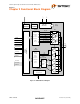
Small Footprint Hi-Speed USB 2.0 Device PHY with UTMI Interface Datasheet Chapter 3 Pinout 1 2 3 4 5 6 7 A RB REN XI XO V33 RXE RXV B XSEL GND V33 V18A VIO GND D0 C TXR TSEL V18 D1 D SPDN TXV D2 D3 E DM RST D4 D5 F DP GND RXA OM0 LS1 GND D6 G V33 V33 OM1 CLK LS0 VIO D7 TOP VIEW Figure 3.1 USB3290 Pinout - Top View Revision 1.
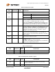
Small Footprint Hi-Speed USB 2.0 Device PHY with UTMI Interface Datasheet Chapter 4 Interface Signal Definition Table 4.1 System Interface Signals NAME DIRECTION ACTIVE LEVEL RESET (RST) Input High Reset. Reset all state machines. After coming out of reset, must wait 5 rising edges of clock before asserting TXValid for transmit. See Section 7.8.3 XCVRSELECT (XSEL) Input N/A Transceiver Select.
Small Footprint Hi-Speed USB 2.0 Device PHY with UTMI Interface Datasheet Table 4.2 Data Interface Signals NAME DIRECTION ACTIVE LEVEL DATA[7:0] (D7) . . . (D0) Bidirectional High TXVALID (TXV) Input DESCRIPTION Data bus. 8-bit Bidirectional mode. TXVALID High DATA[7:0] 0 output 1 input Transmit Valid. Indicates that the DATA bus is valid for transmit. The assertion of TXVALID initiates the transmission of SYNC on the USB bus. The negation of TXVALID initiates EOP on the USB.
Small Footprint Hi-Speed USB 2.0 Device PHY with UTMI Interface Datasheet Table 4.5 Power and Ground Signals NAME DIRECTION ACTIVE LEVEL VDD3.3 (V33) (VIO) N/A N/A 3.3V Supply. Provides power for USB 2.0 Transceiver, UTMI+ Digital, Digital I/O, and Regulators. REG_EN (REN) Input High On-Chip 1.8V regulator enable. Connect to ground to disable both of the on chip (VDDA1.8 and VDD1.8) regulators. When regulators are disabled: External 1.8V must be supplied to VDDA1.8 and VDD1.8 pins.
Small Footprint Hi-Speed USB 2.0 Device PHY with UTMI Interface Datasheet Chapter 5 Limiting Values Table 5.1 Absolute Maximum Ratings PARAMETER SYMBOL CONDITIONS MIN TYP MAX UNITS Maximum DP and DM voltage to Ground VMAX_5V -0.3 5.5 V Maximum VDD1.8 and VDDA1.8 voltage to Ground VMAX_1.8V -0.3 2.5 V Maximum 3.3V Supply Voltage to Ground VMAX_3.3V -0.3 4.0 V Maximum I/O Voltage to Ground VI -0.3 4.
Small Footprint Hi-Speed USB 2.0 Device PHY with UTMI Interface Datasheet Chapter 6 Electrical Characteristics Table 6.1 Electrical Characteristics: Supply Pins (Note 6.1) PARAMETER SYMBOL CONDITIONS Unconfigured Current IAVG(UCFG) Device Unconfigured 55 mA FS Idle Current IAVG(FS) FS idle not data transfer 55 mA FS Transmit Current IAVG(FSTX) FS current during data transmit 60.5 mA FS Receive Current IAVG(FSRX) FS current during data receive 57.
Small Footprint Hi-Speed USB 2.0 Device PHY with UTMI Interface Datasheet Table 6.3 DC Electrical Characteristics: Analog I/O Pins (DP/DM) (Note 6.3) PARAMETER SYMBOL CONDITIONS MIN TYP MAX UNITS FS FUNCTIONALITY Input levels Differential Receiver Input Sensitivity VDIFS Differential Receiver Common-Mode Voltage VCMFS Single-Ended Receiver Low Level Input Voltage VILSE Single-Ended Receiver High Level Input Voltage VIHSE Single-Ended Receiver Hysteresis VHYSSE | V(DP) - V(DM) | 0.
Small Footprint Hi-Speed USB 2.0 Device PHY with UTMI Interface Datasheet Table 6.3 DC Electrical Characteristics: Analog I/O Pins (DP/DM) (Note 6.
Small Footprint Hi-Speed USB 2.0 Device PHY with UTMI Interface Datasheet Table 6.5 Dynamic Characteristics: Digital UTMI Pins (Note 6.5) PARAMETER SYMBOL CONDITIONS MIN TYP MAX UNITS 5 ns UTMI Timing DATA[7:0] TPD Output Delay. Measured from PHY output to the rising edge of CLKOUT 2 TSU Setup Time. Measured from PHY input to the rising edge of CLKOUT. 5 ns TH Hold time. Measured from the rising egde of CLKOUT to the PHY input signal edge.
Small Footprint Hi-Speed USB 2.0 Device PHY with UTMI Interface Datasheet Drive High Iout (mA) Slope = 1/49.5 Ohm -6.1 * |VOH | Test Limit -10.71 * |VOH| Slope = 1/40.5 Ohm 0 0.566*VOH 0 0.698*VOH V OH V out (Volts) Figure 6.1 Full-Speed Driver VOH/IOH Characteristics for High-speed Capable Transceiver Drive Low Iout (mA) Slope = 1/40.5 Ohm Test Limit 10.71 * |VOH| 22 Slope = 1/49.5 Ohm 0 1.09V 0.434*VOH 0 VOH Vout (Volts) Figure 6.
Small Footprint Hi-Speed USB 2.0 Device PHY with UTMI Interface Datasheet 6.2 High-speed Signaling Eye Patterns High-speed USB signals are characterized using eye patterns. For measuring the eye patterns 4 points have been defined (see Figure 6.3). The Universal Serial Bus Specification Rev.2.0 defines the eye patterns in several ‘templates’. The two templates that are relevant to the PHY are shown below.
Small Footprint Hi-Speed USB 2.0 Device PHY with UTMI Interface Datasheet The eye pattern in Figure 6.4 defines the transmit waveform requirements for a hub (measured at TP2 of Figure 6.3) or a device without a captive cable (measured at TP3 of Figure 6.3). The corresponding signal levels and timings are given in table below. Time is specified as a percentage of the unit interval (UI), which represents the nominal bit duration for a 480 Mbit/s transmission rate.
Small Footprint Hi-Speed USB 2.0 Device PHY with UTMI Interface Datasheet The eye pattern in Figure 6.5 defines the receiver sensitivity requirements for a hub (signal applied at test point TP2 of Figure 6.3) or a device without a captive cable (signal applied at test point TP3 of Figure 6.3). The corresponding signal levels and timings are given in the table below. Timings are given as a percentage of the unit interval (UI), which represents the nominal bit duration for a 480 Mbit/s transmission rate.
Small Footprint Hi-Speed USB 2.0 Device PHY with UTMI Interface Datasheet Chapter 7 Functional Overview Figure 2.1 on page 7 shows the functional block diagram of the USB3290. Each of the functions is described in detail below. 7.1 Modes of Operation The USB3290 supports an 8-bit bi-directional parallel interface. 7.
Small Footprint Hi-Speed USB 2.0 Device PHY with UTMI Interface Datasheet Figure 7.2 shows the relationship between CLKOUT and the receive data control signals in FS mode. RXACTIVE "frames" a packet, transitioning only at the beginning and end of a packet. However transitions of RXVALID may take place any time 8 bits of data are available. Figure 7.1 also shows how RXVALID is only asserted for one CLKOUT cycle per byte time even though the data may be presented for the full byte time.
Small Footprint Hi-Speed USB 2.0 Device PHY with UTMI Interface Datasheet The behavior of the Transmit State Machine is described below. 7.5 Asserting a RESET forces the transmit state machine into the Reset state which negates TXREADY. When RESET is negated the transmit state machine will enter a wait state. The SIE asserts TXVALID to begin a transmission. After the SIE asserts TXVALID it can assume that the transmission has started when it detects TXREADY has been asserted.
Small Footprint Hi-Speed USB 2.0 Device PHY with UTMI Interface Datasheet When the EOP is detected the state machine will enter the Strip EOP state and negate RXACTIVE and RXVALID. After the EOP has been stripped the Receive State Machine will reenter the RX Wait state and begin looking for the next packet. The behavior of the Receive State Machine is described below: RXACTIVE and RXREADY are sampled on the rising edge of CLKOUT. In the RX Wait state the receiver is always looking for SYNC.
Small Footprint Hi-Speed USB 2.0 Device PHY with UTMI Interface Datasheet Figure 7.6 Receive Timing for Setup Packet Figure 7.7 Receive Timing for Data Packet (with CRC-16) The receivers connect directly to the USB cable. The block contains a separate differential receiver for HS and FS mode. Depending on the mode, the selected receiver provides the serial data stream through the mulitplexer to the RX Logic block.
Small Footprint Hi-Speed USB 2.0 Device PHY with UTMI Interface Datasheet 7.6 USB 2.0 Transceiver The SMSC Hi-Speed USB 2.0 Transceiver consists of the High Speed and Full Speed Transceivers, and the Termination resistors. 7.6.1 High Speed and Full Speed Transceivers The USB3290 transceiver meets all requirements in the USB 2.0 specification. The receivers connect directly to the USB cable. This block contains a separate differential receiver for HS and FS mode.
Small Footprint Hi-Speed USB 2.0 Device PHY with UTMI Interface Datasheet 7.6.3 Bias Generator This block consists of an internal bandgap reference circuit used for generating the high speed driver currents and the biasing of the analog circuits. This block requires an external 12kΩ, 1% tolerance, external reference resistor connected from RBIAS to ground. 7.
Small Footprint Hi-Speed USB 2.0 Device PHY with UTMI Interface Datasheet Chapter 8 Application Notes The following sections consist of select functional explanations to aid in implementing the USB3290 into a system. For complete description and specifications consult the USB 2.0 Transceiver Macrocell Interface Specification and Universal Serial Bus Specification Revision 2.0. 8.
Small Footprint Hi-Speed USB 2.0 Device PHY with UTMI Interface Datasheet 8.2 OPMODES The OPMODE[1:0] pins allow control of the operating modes. Table 8.
Small Footprint Hi-Speed USB 2.0 Device PHY with UTMI Interface Datasheet 8.4 SE0 Handling For FS operation, IDLE is a J state on the bus. SE0 is used as part of the EOP or to indicate reset. When asserted in an EOP, SE0 is never asserted for more than 2 bit times. The assertion of SE0 for more than 2.5us is interpreted as a reset by the device operating in FS mode. For HS operation, IDLE is a SE0 state on the bus. SE0 is also used to reset a HS device. A HS device cannot use the 2.
Small Footprint Hi-Speed USB 2.0 Device PHY with UTMI Interface Datasheet 8.6 Suspend Detection If a HS device detects SE0 asserted on the bus for more than 3ms (T1), it reverts to FS mode. This enables the FS pull-up on the DP line in an attempt to assert a continuous FS J state on the bus. The SIE must then check LINESTATE for the J condition. If J is asserted at time T2, then the upstream port is asserting a soft SE0 and the USB is in a J state indicating a suspend condition.
Small Footprint Hi-Speed USB 2.0 Device PHY with UTMI Interface Datasheet 8.7 HS Detection Handshake The High Speed Detection Handshake process is entered from one of three states: suspend, active FS or active HS. The downstream facing port asserting an SE0 state on the bus initiates the HS Detection Handshake. Depending on the initial state, an SE0 condition can be asserted from 0 to 4 ms before initiating the HS Detection Handshake. These states are described in the USB 2.0 specification.
Small Footprint Hi-Speed USB 2.0 Device PHY with UTMI Interface Datasheet Figure 8.3 HS Detection Handshake Timing Behavior (FS Mode) Table 8.6 HS Detection Handshake Timing Values (FS Mode) TIMING PARAMETER DESCRIPTION VALUE T0 HS Handshake begins. DP pull-up enabled, HS terminations disabled. 0 (reference) T1 Device enables HS Transceiver and asserts Chirp K on the bus. T0 < T1 < HS Reset T0 + 6.0ms T2 Device removes Chirp K from the bus. 1ms minimum width. T1 + 1.0 ms < T2 < HS Reset T0 + 7.
Small Footprint Hi-Speed USB 2.0 Device PHY with UTMI Interface Datasheet 8.9 HS Detection Handshake – HS Downstream Facing Port Upon entering the HS Detection process (T0) XCVRSELECT and TERMSELECT are in FS mode. The DP pull-up is asserted and the HS terminations are disabled. The SIE then sets OPMODE to Disable Bit Stuffing and NRZI encoding, XCVRSELECT to HS mode, and begins the transmission of all 0's data, which asserts a HS K (chirp) on the bus (T1). The device chirp must last at least 1.
Small Footprint Hi-Speed USB 2.0 Device PHY with UTMI Interface Datasheet Figure 8.5 HS Detection Handshake Timing Behavior (HS Mode) Table 8.7 Reset Timing Values TIMING PARAMETER DESCRIPTION VALUE T0 HS Handshake begins. DP pull-up enabled, HS terminations disabled. 0 (reference) T1 Device asserts Chirp K on the bus. T0 < T1 < HS Reset T0 + 6.0ms T2 Device removes Chirp K from the bus. 1 ms minimum width. T0 + 1.0ms < T2 < HS Reset T0 + 7.
Small Footprint Hi-Speed USB 2.0 Device PHY with UTMI Interface Datasheet Notes: 8.10 T0 may be up to 4ms after HS Reset T0. The SIE must use LINESTATE to detect the downstream port chirp sequence. Due to the assertion of the HS termination on the host port and FS termination on the device port, between T1 and T7 the signaling levels on the bus are higher than HS signaling levels and are less than FS signaling levels.
Small Footprint Hi-Speed USB 2.0 Device PHY with UTMI Interface Datasheet T0 T1 T2 T3 T4 time OPMODE 0 OPMODE 1 XCVRSELECT TERMSELECT SUSPENDN TXVALID CLK60 DP/DM J SE0 CLK power up time Device Chirp K Look for host chirps Figure 8.6 HS Detection Handshake Timing Behavior from Suspend To detect the assertion of the downstream Chirp K's and Chirp J's for 2.5us {TFILT}, the SIE must see the appropriate LINESTATE signals asserted continuously for 165 CLKOUT cycles. Table 8.
Small Footprint Hi-Speed USB 2.0 Device PHY with UTMI Interface Datasheet 8.11 Assertion of Resume In this case, an event internal to the device initiates the resume process. A device with remote wakeup capability must wait for at least 5ms after the bus is in the idle state before sending the remote wake-up resume signaling. This allows the hubs to get into their suspend state and prepare for propagating resume signaling.
Small Footprint Hi-Speed USB 2.0 Device PHY with UTMI Interface Datasheet 8.12 Detection of Resume Resume signaling always takes place in FS mode (TERMSELECT and XCVRSELECT = FS enabled), so the behavior for a HS device is identical to that of a FS device. The SIE uses the LINESTATE signals to determine when the USB transitions from the 'J' to the 'K' state and finally to the terminating FS EOP (SE0 for 1.25us-1.5µs.). The resume signaling (FS 'K') will be asserted for at least 20ms.
Small Footprint Hi-Speed USB 2.0 Device PHY with UTMI Interface Datasheet Figure 8.8 Device Attach Behavior Table 8.10 Attach and Reset Timing Values TIMING PARAMETER DESCRIPTION VALUE T0 Vbus Valid. 0 (reference) T1 Maximum time from Vbus valid to when the device must signal attach. T0 + 100ms < T1 T2 (HS Reset T0) Debounce interval. The device now enters the HS Detection Handshake protocol. T1 + 100ms < T2 Revision 1.
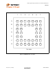
Small Footprint Hi-Speed USB 2.0 Device PHY with UTMI Interface Datasheet 8.14 Application Diagram USB3290 G3 F4 B1 C2 Opmode 1 Opmode 0 D1 E2 SuspendM Reset D2 C1 A7 F3 Txvalid Txready Rxvalid Rxactive A6 F5 G5 Rxerror Linestate 1 G4 Clkout Data0 Data1 Data2 Data3 Data4 Data5 Data6 Xcvrselect 0 Termselect Data7 B7 C7 D6 D7 E6 E7 F7 G7 USB Connector (B) DP F1 DM E1 Linestate 0 DP DM Optional Level Shifter VBUS To VBUS detect input Figure 8.
Small Footprint Hi-Speed USB 2.0 Device PHY with UTMI Interface Datasheet VDD33 G2 VDD33 A5 A2 VDD33 REG_EN B5 VDDIO G6 VDDIO VDDA18 C6 VDD18 A1 RBIAS USB3290 1M 12.0k 0.1uF 4.7uF 0.1uF B4 4.7uF VDD33 G1 B2 B6 F2 F6 A3 30pF* XI GND GND XO GND 24 MHz XTAL 30pF* 0.1uF 4.7uF B3 3.3 Volt Supply A4 GND Figure 8.10 USB3290 Application Diagram showing power and miscellaneous signals Revision 1.
Small Footprint Hi-Speed USB 2.0 Device PHY with UTMI Interface 43 DATASHEET SMSC USB3290 Figure 9.1 USB3290-FH 40 Ball, VFBGA Package Outline & Parameters 4x4x0.9mm Body, Lead-Free RoHS Compliant Datasheet Revision 1.
Small Footprint Hi-Speed USB 2.0 Device PHY with UTMI Interface Datasheet Figure 9.2 BGA, 4x4 Taping Dimensions and Part Orientation Revision 1.
Small Footprint Hi-Speed USB 2.0 Device PHY with UTMI Interface Datasheet Figure 9.3 Reel Dimensions for 12mm Carrier Tape SMSC USB3290 45 DATASHEET Revision 1.
Small Footprint Hi-Speed USB 2.0 Device PHY with UTMI Interface Datasheet Figure 9.4 Tape Length and Part Quantity Note: Standard reel size is 4000 pieces per reel. Revision 1.