
Hardware Description
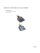
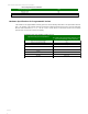


XBee-PRO 900HP Mechanical Drawings
XBee-PRO® 900HP/XBee-PRO® XSC RF Modules
© 2014 7
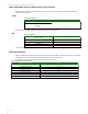
• Signal Direction is specified with respect to the module
• See Design Notes section below for details on pin connections.
XBee-PRO 900HP Design Notes
The XBee modules do not specifically require any external circuitry or specific connections for proper operation. However, there are s ome general design guidelines that are
recommended for help in troubleshooting and building a robust design.
XBee-PRO 900HP Power Supply Design
Poor power supply can lead to poor radio performance, especially if the supply voltage is not kept within tolerance or is exc essively noisy. To help reduce noise, we recommend
placing both a 1^F and 47pF capacitor as near to pin 1 on the PCB as possible. If using a switching regulator for your power supply, switching frequencies above 500kHz are
preferred. Power supply ripple should be limited to a maximum 50mV peak to peak.
Note - For designs using the programmable modules, an additional 10^F decoupling cap is recommended near pin 1 of the module. The nearest proximity to pin 1 of the three caps
should be in the following order: 47pf, 1^F followed by 10^F.
XBee-PRO 900HP Recommended Pin Connections
The only required pin connections are VCC, GND, DOUT and DIN. To support serial firmware updates, VCC, GND, DOUT, DIN, RTS, and DTR should be connected.
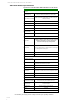
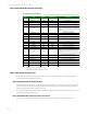
Pin Assignments for XBee Modules
(Low-asserted signals are distinguished with a horizontal line above signal name.)
Pin #
Name
Direction
Default State
Description
1
VCC
Power Supply
2
DOUT/DIO13
Both
Output
GPIO / UART Data out
3
DIN/nConfig/DIO14
Both
Input
GPIO / UART Data In
4
DIO12/SPI_MISO
Both
Output
GPIO / SPI slave out
5
nRESET
Input
Module Reset. Drive low to reset the module. This is also an
output with an open drain configuration with an internal 20 K
ohm pull-up (never drive to logic high, as the module may be
driving it low).
The minimum pulse width is 1 mS.
6
DIO10/PWM0
Both
GPIO / RX Signal Strength Indicator
7
DIO11/PWM1
Both
GPIO / Pulse Width Modulator
8
reserved
Disabled
Do Not Connect
9
nDTR/SLEEP_RQ/DIO8
Both
Input
GPIO / Pin Sleep Control Line (DTR on the dev board)
10
GND
Ground
11
DIO4/AD4/SPI_MOSI
Both
GPIO/SPI slave In
12
nCTS/DIO7
Both
Output
GPIO / Clear-to-Send Flow Control
13
On_nSLEEP/DIO9
Output
Output
GPIO / Module Status Indicator
14
VREF
Input
Internally used for programmable secondary processor. For
compatibility with other XBee modules, we recommend
connecting this pin to the voltage reference if Analog Sampling
is desired. Otherwise, connect to GND.
15
Associate/DIO5
Both
Output
GPIO / Associate Indicator
16
nRTS/DIO6
Both
Input
GPIO / Request-to-Send Flow Control
17
AD3/DIO3/SPI_nSSEL
Both
GPIO / Analog Input / SPI Slave Select
18
AD2/DIO2/SPI_CLK
Both
GPIO / Analog Input / SPI Clock
19
AD1/DIO1/SPI_nATTN
Both
GPIO / Analog Input / SPI Attention
20
AD0/DIO0
Both
GPIO / Analog Input