GR47/GR48 Integrator’s Manual Product Photo/Illustration
The GR47 described in this manual conforms to the Radio and Telecommunications Terminal Equipment (R&TTE) directive 99/5/EC with requirements covering EMC directive 89/336/EEC and Low Voltage directive 73/23/EEC. The product fulfils the requirements according to 3GPP TS 51.010-1, EN 301 489-7 and EN60950. SAR statement: This product is intended to be used with the antenna or other radiating element at least 20 cm away from any part of the human body.
Contents Overview ................................................................................................................... 5 1. Introduction .............................................................................................................. 6 Target Users ................................................................................................................ 6 Prerequisites........................................................................................................
Real Time Clock........................................................................................................ 49 6. Antenna Connector................................................................................................. 51 7. Keyboard Interface ................................................................................................. 52 IO#/KEYROW# ....................................................................................................... 52 KEYCOL# ...............
Overview Product Photo/Illustration
1. Introduction 1.1 Target Users The GR47 and GR48 radio devices are designed to be integrated into machine-to-machine or man-to-machine communications applications. They are intended to be used by manufacturers, system integrators, applications developers and developers of wireless communications equipment. 1.
2. GR47/GR48 RADIO DEVICES 2. GR47/GR48 Radio Devices 2.1 About the GR47/GR48 Family Two radio devices make up the family; GR47 and GR48, for use in the E-GSM900/GSM1800 and GSM850/GSM1900 bands respectively. 1RWH This manual refers to the GR47 and GR48 as radio devices. If there is a difference in the functionality of the radio devices the GR47 and GR48 information will be listed separately.
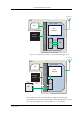
2. GR47/GR48 RADIO DEVICES . GSM NETWORK MS GR47 / GR48 SIM SYSTEM CONNECTOR POWER SUPPLY GSM ENGINE STATUS & RESPONSE DCE EMBEDDED APPLICATION DTE ‘AT’ COMMAND CONTROL Figure 2.1 Main Blocks in a Wireless System (embedded application) GSM NETWORK MS GR47 / GR48 SIM EXTERNAL APPLICATION MS STATUS & RESPONSE SYSTEM CONNECTOR POWER SUPPLY GSM ENGINE DCE DTE DTE ‘AT’ COMMAND CONTROL M Figure 2.
2. GR47/GR48 RADIO DEVICES The functions of the radio device follow the recommendations provided by ETSI (European Telecommunications Standards Institute) and ITU-T. ETSI specifies a set of AT commands for controlling the GSM element of the radio device; these commands are supplemented by Sony Ericsson specific commands. To find out how to work with AT commands, see the AT Commands Manual. 2.
2. GR47/GR48 RADIO DEVICES GR48 GSM 850 GSM 1900 Duplex spacing 45 MHz 80 MHz Receiver sensitivity at antenna connector < –102 dBm < –102 dBm Transmitter output power at antenna connector Class 4 2W (33 dBm) Class 1 1 W (30 dBm) Automatic hand-over between GSM 850 and GSM 1900 2.3.2 Short Message Service The radio device supports the following SMS services: • Sending; MO (mobile-originated) with both PDU (protocol data unit) and text mode supported.
2. GR47/GR48 RADIO DEVICES 2.3.4 Data The radio device supports the following data protocols: • *356 *HQHUDO 3DFNHW 5DGLR 6HUYLFH The radio devices are Class B terminals. The radio devices are GPRS 4+1 enabled, which are capable of receiving at a maximum of four timeslots per frame (down link), and transmitting in one timeslot per frame (up link). • &6' &LUFXLW 6ZLWFKHG 'DWD The radio devices are capable of establishing a CSD communication at 9.6 kbps.
2. GR47/GR48 RADIO DEVICES 2.4 Service and Support 2.4.1 Web Pages Visit our web site for the following information: • where to buy radio devices or for recommendations concerning accessories and components; • the telephone number for customer support in your region; • FAQs (frequently asked questions). The web site address is: http://www.SonyEricsson.com/M2M 2.4.2 Integrator’s Manual This manual provides you with all of the information you need to integrate the radio device into your application. 2.4.
2. GR47/GR48 RADIO DEVICES All the user needs to provide, is a computer or micro-controller and the expertise to use AT commands. 2.5 Precautions The radio devices are ESD protected up to 4K V contact and 8K V air discharge. It is recommended that you follow electronic device handling precautions when working with any electronic device system to ensure no damage occurs to the host or the radio device. In “Integrating the Radio Device”, page 16 you will find more information about safety and product care.
3. ABBREVIATIONS 3.
3.
Integrating the Radio Device Product Photo/Illustration
4. Mechanical Description 4.1 Interface Description The pictures below show the mechanical design of the radio device along with the positions of the different connectors and mounting holes. The radio device is protected with AISI 304 stainless steel covers that meet the environmental and EMC requirements. Figure 4.1 Radio Device viewed from below Figure 4.
4. MECHANICAL DESCRIPTION • Keypad, display, microphone, speaker and battery are not part of the radio device. • The SIM card is mounted in your application, external to the radio device. • The System Connector is a 60-pin, standard 0.05 in (1.27 mm) pitch type. The pins and their electrical characteristics are described in 5. System Connector Interface, page 19. • Information about the Antenna Connector is found in 6. Antenna Connector, page 51. 4.2 Physical Dimensions 2.20 (4x) 2.86 4.78 3.80 2.
5. System Connector Interface 5.1 Overview Electrical connections to the radio device (except the antenna), are made through the System Connector Interface. The system connector is a 60-pin, standard 0.05 in (1.27 mm) pitch device. The system connector allows both board-to-board and board-to-cable connections to be made. Use a board-board connector to connect the radio device directly to a PCB, and a board-cable connector to connect the radio device via a cable. Figure 5.
5. SYSTEM CONNECTOR INTERFACE 1RWH Under the heading “Dir” in the table, radio device input and output signals are indicated by the letters I and O respectively.
5. SYSTEM CONNECTOR INTERFACE Pin Signal Name Dir Signal Type Description 28 ADC3 I Analogue Analogue to digital converter 3 29 SDA I/O 2.75V, internal pull up I 2 C data 30 SCL O 2.75V, internal pull up I 2 C clock 31 BUZZER O Digital 2.75V Buzzer output from radio device 32 OUT3 KEYCOL3 DSR O O O Digital 2.75V General purpose output 3 Keyboard column 3 Data set ready (UART1) 33 LED IO6 O I/O Digital 2.75V Flashing LED General purpose I/O 6 34 VIO O Power Out 2.
5. SYSTEM CONNECTOR INTERFACE Pin Signal Name Dir Signal Type Description 49 PCMO O Digital 2.75V Codec PCM digital audio output 50 PCMI I Digital 2.75V Codec PCM digital audio input 51 PCMSYNC O Digital 2.75V DSP PCM frame sync 52 PCMCLK O Digital 2.
5. SYSTEM CONNECTOR INTERFACE • The SIM output signals and the SIMVCC supply will continuously withstand a short circuit to any voltage within the range 0 V to 4.1V. 5.3 Grounds Pin Signal Description 2, 4, 6, 8, 10, 12 DGND Digital ground 60 AGND Analogue ground There are two ground connections in the radio device, AGND (analogue ground) and DGND (digital ground). Pin assignments are shown in the table above. 1RWH AGND and DGND are connected at a single point inside the radio device.
5. SYSTEM CONNECTOR INTERFACE Connect all VCC pins together in your application in order to carry the current drawn by the radio device. The electrical characteristics for VCC are shown in the table below. Parameter Mode Limit Vcc supply voltage Nominal 3.6 V Tolerance including ripple a 3.4 V - 4.0 V Over-voltage limit 5.
5. SYSTEM CONNECTOR INTERFACE Safety considerations should be taken into account. For example, monitoring the temperature of the battery. If the temperature of the battery exceeds its specification limits, battery charging must be stopped immediately. If the battery temperature continues to rise the application should be suspended or the battery disconnected. 1RWH When charging Lithium batteries, the battery pack must have an internal protection circuit in accordance with the manufacturer’s instructions.
5. SYSTEM CONNECTOR INTERFACE t9,2 Time after start of ON/OFF pulse when VIO is active VCC > 3.2V - 45.0 - ms t38/6( Application ON/ OFF pulse width ON/OFF held low until detected by software 400 500 - ms t3567 Internal Poweron reset signal initiates software 100 - 200 ms t&76 Time when software controlled CTS signal indicates module READY - 0.35 3.
5. SYSTEM CONNECTOR INTERFACE Turning the Radio Device Off tPULSE tOFF ON/OFF VIO tSPD Figure 5.3 Off timings and VIO performance (2) It is a requirement from most GSM network providers that GSM products properly detach from the network during a power-down sequence. In order to achieve this it is important that the VCC supply is not removed or turned off before VIO has been deactivated by the module.
5. SYSTEM CONNECTOR INTERFACE Hard Shutdown Sequence tPULSE ON/OFF tHSD VIO Figure 5.4 Hard Shutdown Sequence Symbol Parameters t+6' Time to complete hardware shutdown t38/6( Application ON/ OFF pulse width Conditions ON/OFF low until VIO is disabled Min. Typ Max Unit 2 - 11 s t+6' 10 - s (4) To implement the Hard Shutdown of the GR47, the ON/OFF pulse must be held low until the sequence is complete. Ensure that ON/OFF is not released before VIO has been deactivated by the module.
5. SYSTEM CONNECTOR INTERFACE 5.7 Analogue Audio Pin Signal Dir Description 57 AFMS O Audio from mobile station 59 ATMS I Audio to mobile station 60 AGND - Ground (return) for analogue audio ATMS is the audio input, and AFMS is the audio output, of the radio device. These signals can be used in car kit mode. There are three factory-set audio profiles: • portable handsfree • handset • car kit Portable handsfree is the factory-set default profile.
5. SYSTEM CONNECTOR INTERFACE The following tables show the nominal PGA (programming gain settings). For more information see the relevant AT commands. Maximum input voltage limit: 245 mVrms Input Input (mVrms) TXAGC (dB) AUX AMP gain PCMOUT (dBm0) ATMS 245 0 13 3 Maximum input level at MICI, 61.4 mVrms output at PCMOUT = 3 dBm0 Input Differential input (mVrms) TXAGC (dB) AUX AMP gain PCMOUT (dBm0) MICN MICP 61.
5. SYSTEM CONNECTOR INTERFACE Parameter Limit Output Capacitance 2.2 µF ±10 % Levels (THD < 5 %) Drive capability into 5 kΩ (0.3 - 3.5 kHz) > 2.4 Vp-p Drive capability into 1.5 kΩ (0.3 - 3.5 kHz) > 2.2 Vp-p Drive capability into 150 Ω (at 1 kHz) > 1.3 Vp-p 5.7.3 Microphone Signals Pin Speaker signals Dir Function 53 MICP I Microphone positive input 54 MICN I Microphone negative input MICP and MICN are balanced differential microphone input pins.
5. SYSTEM CONNECTOR INTERFACE 5.7.4 Speaker Signals Pin Speaker signals Dir Function 55 BEARP O Speaker positive output 56 BEARN O Speaker negative output BEARP and BEARN are the speaker output pins. These are differential-mode outputs. The electrical characteristics are given in the table below. Parameter Limit Output level (differential) ≥ 4.0 VSS Output level (dynamic load = 32 Ω) ≥ 2.
5. SYSTEM CONNECTOR INTERFACE 5.8 PCM Digital Audio Pin Signal Dir Function 52 PCMCLK O PCM clock 51 PCMSYNC O PCM frame sync 47 PCMULD I PCM audio input to DSP 48 PCMDLD O PCM audio output from DSP 50 PCMIN I PCM audio input to Codec 49 PCMOUT O PCM audio output to Codec Figure 5.6 shows the PCM (Pulse Code Modulation) digital audio connection for external devices.
5. SYSTEM CONNECTOR INTERFACE 5.8.1 PCM Data Format All of the radio device’s PCM signals, including signals between its CODEC and DSP conform to the PCM data I/O format of the industry standard DSP from Texas Instruments. PCMCLK (bit clock) and PCMSYNC (frame synchronisation) are both generated by the DSP within the radio device.
5. SYSTEM CONNECTOR INTERFACE PCM Timing Diagrams The PCM timing is shown in Figure 5.8 below and it is seen that the CPU has 45 µs to serve an interrupt and setup data channels. Data is sent on the falling edge of the sync pulse. The data bits in PCMULD and PCMDLD are aligned so that the MSB in each word occurs on the same clock edge as shown in Figure 5.9. 125 µs Clk Sync 45 µs Data Figure 5.8 16-bit word within 24-bit frame PCM signal timing is shown in Figure 5.9.
5. SYSTEM CONNECTOR INTERFACE Typical Rise/Fall times Rise Time Fall Time Unit PCMCLK 19 18 ns PCMSYN 19 15 ns PCMOUT 900 900 ns PCMDLD 20 19 ns 5.
5. SYSTEM CONNECTOR INTERFACE Digital 2.75 V CMOS input/output electrical characteristics apply. The standard character format consists of 1 start bit, 8 bit data, no parity and 1 stop bit. In all, there are 10 bits per character. 5.9.1 UART1 (RS232) - RD, TD, RTS, CTS, DTR, DSR, DCD and RI UART1 signals conform to a 9-pin RS232 (V.24) serial port. 1RWH UART1 signal levels do not match standard RS232 (V.28) levels. The relationship between the levels is shown in the table below.
5. SYSTEM CONNECTOR INTERFACE 5.9.3 Control Signals - RTS, CTS, DTR, DSR, DCD, RI UART1 control signals are active low and need a standard interface IC, such as the MAX3237, to generate standard RS232 levels. UART1 converted signals, together with DGND, RD and TD form a 9-pin RS232 data port. RTS and CTS are capable of transmitting at 1/10th of the data transmission speed for data rates up to 460 kbit/s (byte-oriented flow control mechanism).
5. SYSTEM CONNECTOR INTERFACE Data Terminal Ready (DTR) DTR indicates that the DTE is ready to receive data. It also acts as a hardware ‘hang-up’, terminating calls when switched high. The signal is active low. You can define the exact behaviour of DTR with an AT command. Data Set Ready (DSR) DSR indicates that the DCE is ready to receive data. The signal is active low. Data Carrier Detect (DCD) DCD indicates that the DCE is receiving a valid carrier (data signal) when low.
5. SYSTEM CONNECTOR INTERFACE 5.9.5 UART3 - TD3, RD3 UART3 is a full duplex serial communication port with transmission and reception lines. It has the same timing and electrical signal characteristics as UART1, TD and RD. Transmitted Data 3 (TD3) TD3 is used by your application to send data to the radio device via UART3. Received Data 3 (RD3) RD3 is used to send data to your application via UART3. 5.
5. SYSTEM CONNECTOR INTERFACE Signal Parameter Mode Min. SIMDAT High Level Output voltage (V ) 3V 2+ SIMDAT Low Level Output voltage (V ) 2/ SIMCLK SIMRST High Level Output voltage (V ) SIMCLK SIMRST Low Level Output voltage (V ) 2+ 2/ Typ. Max. Unit 2.7 3.0 V 5V 4.7 5.0 V 3V 0 0.2 V 5V 0 0.2 V 3V 2.4 3.0 V 5V 4.4 5.0 V 3V 0 0.35 V 5V 0 0.3 V 5.10.
5. SYSTEM CONNECTOR INTERFACE The electrical characteristics are given below. The signal reference is DGND. Mode SERVICE Voltage (V) Min. Typ. Normal Operation Service/enable programming 1.9 2.75V Absolute maximum voltage Drive Capacity Max. 0.8 - 3.6 > 1 mA 13.5 5.
5. SYSTEM CONNECTOR INTERFACE The following circuit can be used to connect an LED. VCC 330 LED GR47/48 DGND 10k BC817 10k Figure 5.10 Electrical connections for the LED 5.
5. SYSTEM CONNECTOR INTERFACE The operational modes of multiplexed signals are controlled by AT commands and also by intrinsic functions available to an embedded The following table gives you the input impedance. These values only apply when the ports are configured as input signals. 1RWHV Parameter Min. Typ. Max. Units Input impedance (pull-up) 50 100 120 kΩ I/O6 (LED) doesn’t have an internal pull up. If this pin is configured as an input, it should not be left floating.
5. SYSTEM CONNECTOR INTERFACE 5.15.2 I#/O# If pins labelled I# and O# are not being used for an alternative function they may be used for general purpose inputs or outputs respectively. The inputs have an on-board 100k pull-up resistor and the outputs are driven rail-to-rail at 2.75V levels. 5.15.3 UART3/IO# The UART3 pins have been given alternative functions as general purpose I/O, both pins may be used for either input or output.
5. SYSTEM CONNECTOR INTERFACE 5.16.1 Digital to Analogue Converter - DAC The DAC is an 8-bit converter. Conversion takes place when an AT command is sent to the radio device. The radio device sends the resulting analogue value to the DAC pin. Tolerance on this internal voltage is ± 5 % DAC output electrical characteristics are given in the following table. Parameter Limit Units Resolution 8 Bits Output voltage for code = 0 (2.75(6) x 0.05) ± 0.05 V Output voltage for code = 255 (2.75(6) x 0.
5. SYSTEM CONNECTOR INTERFACE 5.16.2 Analogue to Digital Converters 1, 2 and 3 - ADCx The ADC is an 8-bit converter. An analogue value applied to any of the ADC pins is converted and stored in a register inside the radio device. When the appropriate AT command is received by the radio device, the digital value stored in the register is read. ADC electrical characteristics are shown in the table below. (9) Tolerance on this internal voltage is ±5% 5.16.
5. SYSTEM CONNECTOR INTERFACE 1RWH If the voltage of the signal to be measured may be altered by the internal circuitry of this shared signal, then the application should use ADC1, ADC2 or ADC3 instead. 2.75V 2.75V 1MΩ 100kΩ 10kΩ A ADC 10#/ADC# 1nF Analog IC Figure 5.12 Input circuit for combined digital I/O and ADC pins 5.
5. SYSTEM CONNECTOR INTERFACE Parameter Min. Typ. Receive operation Frequency I 2 C CLK Max. Units 400 kHz High or low I 2 C CLK 1.2 µs Delay time after falling edge of I 2 C CLK 100 ns Hold time after falling edge of I 2 C CLK 0 ns 5.18 TX_ON - Burst Transmission Pin Signal Dir Description 35 TX_ON O GSM radio device to transmit Burst transmission is the time when a GSM transceiver unit is transmitting RF signals. TX_ON indicates the radio device is going into transmission mode.
5. SYSTEM CONNECTOR INTERFACE In back-up mode, the back-up source must provide enough power for RTC operation. Refer to the table for the amount of current required. The following table shows voltage characteristics for both modes. Parameter Min. Typ. Max. Units Supply Voltage RTC (normal mode charging the capacitor) 1.6 1.8 2.0 V Supply Voltage RTC (back-up mode Capacitor provides the current) 1.0 1.8 2.0 V 5.0 10.0 µA Current drawn If the voltage drops below 1.
6. ANTENNA CONNECTOR 6. Antenna Connector The radio device’s antenna connector allows transmission of the radio frequency (RF) signals from the radio device to an external customersupplied antenna. The connector is a micro-miniature coaxial MMCX surface mounted component. A number of suitable MMCX type, mating plugs are available from the following manufacturers; • Amphenol; • Suhner; • IMS Connector Systems. The nominal impedance of the antenna interface is 50Ω.
7. KEYBOARD INTERFACE 7. Keyboard Interface To increase I/O capabilities, the radio device optimises the I/O by multiplexing or sharing different features on single pins. The I/O has been extended to allow simple interfacing of a matrix keypad. 7.1 IO#/KEYROW# When configured for keypad operation the software will configure the digital I/O pins as input or high impedance tri-state. In this state, the keypad matrix row can be read from the KEYROW# inputs. These pins have a 100kΩ pull-up to 2.
7. KEYBOARD INTERFACE The method of connection is shown below. KEYROW# GR47 1 2 3 4 5 6 RN1107 KEYCOL# RN1107 RN1107 Figure 7.1 Keyboard matrix connections 1RWH This matrix pattern may be repeated up to 5 columns and 4 rows (one column will use a ground connection as a virtual column driver).
8. HINTS FOR INTEGRATING THE RADIO DEVICE 8. Hints for Integrating the Radio Device This chapter gives you advice and helpful hints on how to integrate the radio device into your application from a hardware perspective. Please read and consider the information under the following headings before starting your integration work: • Safety advice and precautions. • Installation of the radio device. • Antenna. 8.1 Safety Advice and Precautions 8.1.
8. HINTS FOR INTEGRATING THE RADIO DEVICE 8.1.2 SIM Card • Before handling the SIM card in your application, ensure that you are not charged with static electricity. Use proper precautions to avoid electrostatic discharges. The radio device must be switched off before the SIM card is installed in your application. • When the SIM card hatch is opened, the SIM card connectors lie exposed under the SIM card holder.
8. HINTS FOR INTEGRATING THE RADIO DEVICE 8.2 Installation of the Radio Device 8.2.1 Where to Install the Radio Device There are several conditions which need to be taken into consideration when designing your application as they might affect the radio device and its function. They are: Environmental Conditions The radio device must be installed so that the environmental conditions stated in the Technical Data chapter, such as temperature, humidity and vibration are satisfied.
8. HINTS FOR INTEGRATING THE RADIO DEVICE • If you intend to use SMS in the application, ensure this is included in your (voice) subscription. • Consider the choice of the supplementary services described in section 2.3.2 Short Message Service, page 10. 8.2.2 How to Install the Radio Device Power Supply • Use a high-quality power supply cable with low resistance. This ensures that the voltages at the connector pins are within the allowed range, even during the maximum peak current.
8. HINTS FOR INTEGRATING THE RADIO DEVICE 8.3 Antenna 8.3.1 General The antenna is the component in your system that maintains the radio link between the network and the radio device. Since the antenna transmits and receives electromagnetic energy, its efficient function will depend on: • the type of antenna (for example, circular or directional); • the placement of the antenna; • communication disturbances in the vicinity in which the antenna operates.
8. HINTS FOR INTEGRATING THE RADIO DEVICE In general, CE-marked products for residential and commercial areas, and light industry can withstand a minimum of 3 V/m. 8.3.4 The Antenna Cable Use 50 Ω impedance low-loss cable and high-quality 50 Ω impedance connectors (frequency range up to 2 GHz) to avoid RF losses. Ensure that the antenna cable is as short as possible. The Voltage Standing-Wave Ratio (VSWR) may depend on the effectiveness of the antenna, cable and connectors.
9. EMBEDDED APPLICATIONS 9. Embedded Applications The radio device has the capability to store and run customer written code in the form of a script during the processor’s idle time, through the use of an on board interpreter. 9.1 Features Main features of embedded applications are as follows.
9. EMBEDDED APPLICATIONS 9.2.2 M2mpower IDE (Integrated Development Environment) The IDE is a Windows based package which allows the user to write, simulate, debug and download the application into a radio device with the embedded application (EA) software. The standard version is designed to run on Windows XP and 2000, other versions are available for 98 if required.
10. TCP/IP STACK 10. TCP/IP Stack An on board IP/TCP/UDP stack has been integrated into the software negating the need for the customer to implement one in their own code base. This is only accessible by using an embedded applications (see section 9) using intrinsic functions. 10.1 Implementation The following types of commands allow various functions: • Open/closing IP connection - Negotiates/closes a dynamic IP address with the web server.
11. TECHNICAL DATA 11. Technical Data Mechanical Specifications Maximum length 50 mm Maximum width 33 mm Maximum thickness 6.82 mm(excluding connector pins and top of antenna connector) Weight 18.5 g Power supply voltage, normal operation Voltage 3.6 V nominal (3.4 V - 4.
11. TECHNICAL DATA Environmental specifications Operating temperature range (full specification) -10 °C to +55 °C Operating temperature range (working) -30 °C to +75 °C Storage temperature range -40 °C to +85 °C Maximum relative humidity 95 % at +40 °C Stationary vibration, sinusoidal Displacement: 7.5 mm Acceleration amplitude: 20 m/s² and 40 m/s² Frequency range: 2-8 Hz, 8-200 Hz, 200-500 Hz Stationary vibration, random Acceleration spectral density (m²/s²): 0.96, 2.88, 0.
12. DECLARATION OF CONFORMITY 12.
Developer’s Kit Product Photo/Illustration
13. Introduction to the Developer’s Kit The developer’s kit for the radio devices is designed to get you started quickly. It contains all the hardware you will need to begin the development of an application. The only items you need to provide are; a computer, a SIM card and network subscription, and a knowledge of programming with AT commands. 1RWH Before connecting up and using the developer’s kit, we strongly recommend you read “Integrating the Radio Device”, page 16 and all of this section.
13. INTRODUCTION TO THE DEVELOPER’S KIT 13.2 General Functioning of the Kit The following block diagrams are provided to help you understand the general principles of operation of the developer’s kit. You can use the kit’s connectors to access and control the radio device (all switches and jumpers in their default positions). Figure 13.1 shows the various on-board voltages and how they are fed to the radio device and other circuitry.
13. INTRODUCTION TO THE DEVELOPER’S KIT Figure 13.2, Figure 13.3 and Figure 13.4 show how various signals are routed on the developer’s board. Thicker lines indicate multiple signals. X3 X2 3V6 VIO On/Off On/Off & PSU Control GPIO X1 Status LED LED DAC / ADC 1 - 5 I2C I2C GPIO TX_ON SIM SIM Header VRTC SIM Figure 13.2 Miscellaneous signals, connection and routing ATMS MIC 3.5mm socket AFMS EAR 3.
13. INTRODUCTION TO THE DEVELOPER’S KIT X3 X2 DSR, RI, DTR, CTS, RTS, DCD X1 UART1 Flow Control TD, RD TD2, RD2 UART TD3, RD3 SERVICE SERVICE LED Figure 13.
14. USING THE DEVELOPER’S KIT 14. Using the Developer’s Kit This section provides you with the information needed to setup and use the developer’s kit. Before changing switch and jumper settings, refer to “14.3 Jumpers”, page 74. Front and rear views of the developer’s kit are shown below. Use a flat blade screwdriver to unhinge the side clips of the kit and lift the plastic lid off to access the inside. EXT VCC RF Figure 14.1 Front view Figure 14.
14. USING THE DEVELOPER’S KIT 14.1 Start up Check List To use the developer’s kit in standard format check the following: • With the case lid removed, make sure the radio device is plugged into X1 and the RF lead is connected to the MMCX socket of the radio device; • Add your SIM card; • Check the jumpers are in their default positions. Refer to Figure 14.
14. USING THE DEVELOPER’S KIT 14.2 Developer’s Board Overlay D21 Figure 14.3 shows the developer’s board, including the position of all the connectors, switches and jumpers (default positions).
14. USING THE DEVELOPER’S KIT 14.3 Jumpers All jumpers are located on the developer’s board (see “Developer’s board overlay”, page 73). 3RZHU DQG &RQWURO Jumper Default Description INT/EXT INT Selects which voltage path supplies the DK support circuitry (not the supply to the radio device). INT selects power from the internal +3.6V DC supply. EXT selects power from the EXT VCC connector.
14. USING THE DEVELOPER’S KIT Jumper Default Description DIS - When fitted, the serial port driver IC disables the receiver buffers that normally drive UART signals into the radio device. This will prevent the radio device from receiving data through the serial port. WAKE - When fitted, the radio device will automatically power-up when the UART DTR signal is driven high. This allows a convenient mechanism for an external host computer to switch on the module.
14. USING THE DEVELOPER’S KIT $XGLR DQG 3&0 Jumper Default Description ULD To OUT To enable analog audio microphone path ULD must be connected to OUT using the jumper. OUT To ULD To enable analog audio microphone path OUT must be connected to ULD using the jumper. DLD To IN To enable analog audio earpiece path DLD must be connected to IN using the jumper. In To DLD To enable analog audio earpiece path IN must be connected to DLD using the jumper.
14. USING THE DEVELOPER’S KIT DCD Fitted Connects serial port control signal DCD between UART connector X4 and radio device. Note: DCD is a dual function signal from the radio device. When this signal is being used for any other purpose (e.g. Keypad or application specific through X2 or X3), this jumper must be removed. TD Fitted Connects serial port Transmit Data signal TD between UART connector X4 and radio device. Note: It is only valid to have one Transmit Data buffer in the circuit.
14. USING THE DEVELOPER’S KIT 14.4 Switches All switches are mounted on the front panel of the developer’s box. Switch Default Description Vcc (SW1) N/C This switch chooses the voltage source that the radio device will use. The default state N/C makes the voltage path to the radio device open circuit. Choosing INT connects the internal +3.6V DC supply to the VCC pins of the radio device. Choosing EXT connects the external +3.6V DC supply to the VCC pins of the radio device. Note: The external +3.
14. USING THE DEVELOPER’S KIT 14.5 Headers Header Connections Description PCM ULD, DLD, OUT, IN, SYN, CLK Carries digital audio PCM signals for access by user application. Note: In order for analog audio to be created internally by the radio device, signal ULD must be connected to OUT for the MIC path and signal DLD must be connected to IN for the EAR path. SIM VCC, RST, CLK, VPP, DAT, PR#, GND This connector allows access to the SIM interface signals.
14. USING THE DEVELOPER’S KIT 14.6 Connectors Connector Type Description RADIO DEVICE ‘X1’ 60 PinDual Row0.05” pitch The radio device is 'plugged-in' to the development kit. This allows direct connection of the module to the development board. APPLICATION ‘X2’ 40 PinDual Row0.1” pitch This 40-pin connector is compatible with standard 0.1" pitch mating connectors and with 0.05" pitch IDC ribbon cable connectors. This allows the user a range of connection methods to interface to the application.
14. USING THE DEVELOPER’S KIT Connector Type Description Handset ‘X6’ RJ9 socket Connector for a standard telephone handset. Carries signals from the balanced outputs BEARN and BEARP and to the balanced inputs MICN and MICP. To enable an analog audio link it is necessary to link PCM signals “ULD to OUT” and “DLD to IN” using jumper links on the PCM header. Note: The PCM links to enable analog audio are fitted by default but may have been removed during customer development.
14. USING THE DEVELOPER’S KIT Connector Type Description EXT VCC 3 pin Circular This connector carries three signals: EXT VCC (1); CHG_IN (3); GND (2). (These signals are wired into PCB holes labelled EXT, CHG, GND 1 2 respectively).EXT VCC must be a +3.6VDC source capable of 3 supplying up to 2.0A. This can be a battery source.CHG_IN can be a +5.0VDC source capable of supplying 600mA maximum.GND is the ground reference to be used by the external supplies.
14. USING THE DEVELOPER’S KIT 14.8 System Connector Pin Assignments Refer to the table below when monitoring signals on, or connecting to, X1. The table shows the system-connector pin assignments for the radio devices. See “System Connector Interface”, page 19for more details.
D21 14. USING THE DEVELOPER’S KIT INT EXT U8 ULD DLD OUT IN SYN CLK 2 60 PCM X5 59 +3.6V internal power supply 1 BUZZER SIM CHG GND EXT SW2 UART X9 SW1 Audio A0 A1 A2 Buzzer GND PR# DAT GND RST CLK VPP VCC 39 TD DCD RTS CTS DTR RI LED DSR SIM INT 1 X2 X3 Application interface Keypad interface C2 R3 C3 R4 C4 P0 P1 P2 P3 I2C to GPIO X1 pin numbering viewed from the front of the developer's kit. Figure 14.