
Integrator's Manual GR47/GR48


5. SYSTEM CONNECTOR INTERFACE
21
LZT 123 7589 R1A
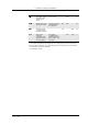
28 ADC3 I Analogue Analogue to digital converter 3
29 SDA I/O 2.75V, internal
pull up
I
2
C data
30 SCL O 2.75V, internal
pull up
I
2
C clock
31 BUZZER O Digital 2.75V Buzzer output from radio device
32 OUT3
KEYCOL3
DSR
O
O
O
Digital 2.75V General purpose output 3
Keyboard column 3
Data set ready (UART1)
33 LED
IO6
O
I/O
Digital 2.75V Flashing LED
General purpose I/O 6
34 VIO O Power Out
2.75 V
Radio device power indication. VIO is a
2.75 V at 75 mA output supply that can
be used to power external circuitry that
interfaces to the radio device
35 TX_ON O Digital 2.75V This output indicates when the GSM
radio device is going to transmit the
burst
36 RI
KEYCOL2
O2
O
O
O
Digital 2.75V Ring Indicator (UART1)
Keyboard column 2
General purpose output 2
37 DTR
KEYROW1
IN1
I
I
I
Digital 2.75V Data Terminal Ready (UART1)
Keyboard row 1
General purpose input 1
38 DCD
KEYCOL1
O1
O
O
O
Digital 2.75V Data Carrier Detect (UART1)
Keyboard column 1
General purpose output 1
39 RTS
IO9
I
I/O
Digital 2.75V Request To Send (UART1)
General purpose I/O 9
40 CTS
KEYCOL4
O4
O
O
O
Digital 2.75V Clear To Send (UART1)
Keyboard column 4
General purpose output 4
41 TD I Digital 2.75V Transmitted Data (UART1).
Data from DTE (host) to DCE (radio
device).
42 RD O Digital 2.75V Received Data (UART1).
Data from DCE (radio device) to DTE
(host).
43 TD3
I/O7
I
I/O
Digital 2.75V Transmitted data (UART3)
General purpose I/O 7
44 RD3
I/O8
O
I/O
Digital 2.75V Received data (UART3)
General purpose I/O 8
45 TD2 I Digital 2.75V Transmitted data (UART2).
Used for flashing the memory.
46 RD2 O Digital 2.75V Received data (UART2).
Used for flashing the memory.
47 PCMULD I Digital 2.75V DSP PCM digital audio input
48 PCMDLD O Digital 2.75V DSP PCM digital audio output
Pin Signal Name Dir Signal Type Description