
Integrator's Manual GR47/GR48


5. SYSTEM CONNECTOR INTERFACE
24
LZT 123 7589 R1A
Connect all VCC pins together in your application in order to carry the
current drawn by the radio device.
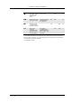
The electrical characteristics for VCC are shown in the table below.
1RWH The radio device has no internal capacitance to supply the large current
peaks during GSM burst transmission. We recommend you follow these
general guidelines:
• Fit a low ESR electrolytic capacitor close to the radio device:
> 1,000 µF;
< 100 m
Ω ESR.
• Make sure power supply to radio device line resistance is < 200 m
Ω.
5.5 Battery Charging Input (CHG_IN)
For battery powered applications, the radio device has a connection to aid
and support battery charging. The typical design where this may be
applicable is to power the radio device directly from a battery source
connected to VCC (pins 1, 3, 5, 7, 9) and to provide a 5V dc power source
(600mA max) to the CHG_IN connection (pin 11). The radio device can
control an internal switching FET which creates a charging pathway to the
battery. While power is provided at CHG_IN, the battery charge can be
maintained. If the power should fail or be removed at CHG_IN, the
application will be supported by the battery alone. When CHG_IN
voltage returns, the battery charging and maintenance will commence once
more.
&DXWLRQ Battery charging algorithms are unique to different battery types. Sony
Ericsson Mobile Communications will not accept any responsibility or
liability for damage, product failures, even death or injury occurring as a
result of incompatible battery and charging algorithms being applied
without their prior knowledge and consent.
Parameter Mode Limit
Vcc supply voltage
Nominal 3.6 V
Tolerance
including ripple
a
a. Measured at system connector pins.
3.4 V - 4.0 V
Over-voltage limit 5.5 V
Maximum ripple < 100 mV @ <200 kHz;
< 20 mV @ > 200 kHz
Maximum allowable voltage
drop
Burst transmission 200 mV
Current drawn, at full TX
power
< 500 mA (average)
< 2 A (peak)