
Integrator's Manual GR47/GR48


13. INTRODUCTION TO THE DEVELOPER’S KIT
68
LZT 123 7589 R1A
13.2 General Functioning of the Kit
The following block diagrams are provided to help you understand the
general principles of operation of the developer’s kit.
You can use the kit’s connectors to access and control the radio device (all
switches and jumpers in their default positions).
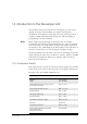
Figure 13.1 shows the various on-board voltages and how they are fed to
the radio device and other circuitry. The developer’s board is powered by
an external power supply connected to Vcc, see below. The power to the
so.4(rce.t)]TJ/92 1 Tf13.69 52817 TD0.0012 Tc-0.0012 Tw[(Figure 13.1 Ppower supply )-8.1boonnecio