
Integrator's Manual GR47/GR48


13. INTRODUCTION TO THE DEVELOPER’S KIT
69
LZT 123 7589 R1A
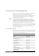
Figure 13.2, Figure 13.3 and Figure 13.4 show how various signals are
routed on the developer’s board. Thicker lines indicate multiple signals.
Figure 13.2 Miscellaneous signals, connection and routing
Figure 13.3 Audio signals, connection and routing
X3
X2
X1
Status LED
On/Off
SIM
SIM
Header
I
2
C
GPIO
3V6
VIO
On/Off &
PSU Control
GPIO
LED
DAC/ADC1-5
I
2
C
TX_ON
SIM
VRTC
AFMS
EAR
3.5mm socket
ATMS
MIC
3.5mm socket
PCM
PCM
6 pin header
BUZZER
Buzzer
MICN, MICP, BEARN, BEARP
RJ9 connector
Handset
X1