
Modem User Manual

LZT 123 1834 34
5.3 General Electrical and Logical Characteristics
The core digital IO is based upon 1.8V technology in the baseband chipset. All
external IO signals undergo bi-directional level shifting on the physical module to
provide flexibility to users of different voltage technology. An internal core IO
regulator is used as a reference for the module-side logic, whilst the application
(host-side) reference is fed by VREF in one of two implementations.
In order to provide legacy users a migration path to GR64, the module IO is made
compatible with 2.8V (or level-adapted 3.0V) controllers, popular in older technology
applications. This arrangement is implemented in variant products DPY 102
1494/10 & DPY 102 1494/30. In these products the 2.8V VREF is derived from an
internal voltage regulator, distributed to the host-side level shifters and also output
on the VREF signal pin.
The arrangement differs in non-legacy variant GR64 products DPY 102 1494/20 &
DPY 102 1494/40. In these products the internal voltage regulator is disconnected
and the user application provides the VREF as a reference to the host-side level
shifters.
The range of VREF voltages is specified in sections 5.6.1 & 5.6.2.
Many of the signals indicated in Table 5.1-1 are high-speed CMOS
logic inputs or outputs powered by the 1.8V internal core regulators,
and then subsequently level shifted at the system interface. All serial
interfaces and general purpose IO fall in to this category.
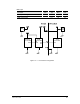
5.3.1 Level Shifter Interfaces
Two different level shifter circuits are implemented in GR64. The ‘common’ interface
is used on all level-shifted IO with the exception of the I
2
C signals, SDA & SCL.
5.3.1.1 Common Level Shifter Interface
The common level shifter used within the GR64 is a Maxim MAX3001EEBP-T, which
has a specified maximum data rate of 4Mbps. The level shifter has ESD protection to
±15kV (HBM).
NOTE