SCD-XA5400ES SERVICE MANUAL US Model Canadian Model AEP Model Ver. 1.0 2008.08 Model Name Using Similar Mechanism NEW Mechanism Type CDM66F-DVBU101 Optical Pick-up Block Name KHM-313CAB SPECIFICATIONS When a Super Audio CD is played General Output jacks Playing frequency range 2 Hz to 100 kHz Frequency response 2 Hz to 50 kHz (–3 dB) Dynamic range 110 dB or more Total harmonic distortion rate 0.0012 % or less Wow and flutter Value of measurable limit (±0.001 % W.
SCD-XA5400ES NOTES ON CHIP COMPONENT REPLACEMENT • Never reuse a disconnected chip component. • Notice that the minus side of a tantalum capacitor may be damaged by heat. FLEXIBLE CIRCUIT BOARD REPAIRING • Keep the temperature of soldering iron around 270 °C during repairing. • Do not touch the soldering iron on the same conductor of the circuit board (within 3 times). • Be careful not to apply force on the conductor when soldering or unsoldering.
SCD-XA5400ES TABLE OF CONTENTS 1. SERVICING NOTES ............................................. 4 2. GENERAL .................................................................. 6 3. DISASSEMBLY 3-1. 3-2. 3-3. 3-4. 3-5. 3-6. 3-7. 3-8. Disassembly Flow ........................................................... Case ................................................................................. Loading Panel Assy ........................................................ Front Panel Assy ............
SCD-XA5400ES SECTION 1 SERVICING NOTES NOTES ON HANDLING THE OPTICAL PICK-UP BLOCK OR BASE UNIT The laser diode in the optical pick-up block may suffer electrostatic break-down because of the potential difference generated by the charged electrostatic load, etc. on clothing and the human body. During repair, pay attention to electrostatic break-down and also use the procedure in the printed matter which is included in the repair parts. The flexible board is easily damaged and should be handled with care.
SCD-XA5400ES HOW TO OPEN THE TRAY WHEN POWER SWITCH TURNS OFF " # – BOTTOM VIEW – cam (66) Pull out the tray in the direction of arrow #. Rotate the cam (66) with a tapering driver in the direction of arrow ". MAIN BOARD SERVICE POSITION In checking the MAIN board, prepare jig (extension cable J-2501-102-A: 1 mm Pitch, 13 cores, Length 300 mm). AUDIO board (CN151) connect jig (extension cable J-2501-102-A) to MAIN board (CN501, CN1100) and AUDIO board (CN151, CN152).
SCD-XA5400ES SECTION 2 GENERAL This section is extracted from instruction manual. Front Panel " / (power) switch Turns the power of the player on or off. To let the player enter power-saving mode (standby mode), press =/ (power) on the remote or on the player. # TIME/TEXT button Switches the playing time of the track, the remaining time of the disc, or TEXT information on the display.
SCD-XA5400ES Remote # SA-CD/CD button Switches between the Super Audio CD layer and the CD layer of a hybrid disc. $ HDMI button Sets whether the audio signal is output from the HDMI OUT jack or not. % REPEAT button Performs Repeat Play. Inserting batteries into the remote Insert two R6 (size-AA) batteries into the battery compartment with the + and – correctly oriented to the markings. When using the remote, point it at the remote sensor on the player. & SHUFFLE button Performs Shuffle Play.
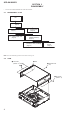
SCD-XA5400ES SECTION 3 DISASSEMBLY • This set can be disassembled in the order shown below. 3-1. DISASSEMBLY FLOW SET 3-2. CASE (Page 8) 3-3. LOADING PANEL ASSY (Page 9) 3-4. FRONT PANEL ASSY (Page 9) 3-5. MAIN BOARD (Page 10) 3-6. MECHANISM DECK (CDM66F-DVBU101) (Page 10) 3-7. MOTOR BOARD, MOTOR (L) ASSY (LOADING) (Page 11) 3-8. BASE UNIT BLOCK (Page 11) Note: Follow the disassembly procedure in the numerical order given. 3-2.
SCD-XA5400ES 3-3. LOADING PANEL ASSY Pull out the tray in the direction of arrow #. loading panel assy two screws (BVTP2.6 (3CR)) # " – BOTTOM VIEW – cam (66) Rotate the cam (66) with a tapering driver in the direction of arrow ". 3-4.
SCD-XA5400ES 3-5. MAIN BOARD connector (CN506, CN1201, CN1202) six screws (BVTP3 × 8) wire (flat type) (24 core) (CN1101) R MAIN board wire (flat type) (13 core) (CN1100) wire (flat type) (19 core) (CN502) wire (flat type) (13 core) (CN501) two screws (BVTP3 × 8) screw (B3 × 6) 3-6.
SCD-XA5400ES 3-7. MOTOR BOARD, MOTOR (L) ASSY (LOADING) belt (LD) gear (LD) two screws (B2.6 × 4) connector (CN012) cushion two claws tray (66F) RB motor (L) assy (loading) Remove two solders. R MOTOR board 3-8. BASE UNIT BLOCK – BOTTOM VIEW – cam (66) base unit block floating screw (DIA.
SCD-XA5400ES SECTION 4 TEST MODE Note 1: According to the following procedures when you ship it (Return it to the customer). 1. SERVICE MODE of step 6 and 7 (DVD EEPROM clearness) 2. COLD RESET Note 2: “DVD” displayed by the test mode shows "super audio CD”. COLD RESET The cold reset clears data stored in microcomputer’s RAM to initial conditions. Procedure: 1. Press three buttons of [x], [A] and [?/1] on the set simultaneously. 2. “COLD RESET” appears on the fluorescent indicator tube.
SCD-XA5400ES List of trouble log Note: “nnn” of toggle article number is a generation frequency of the error.
SCD-XA5400ES DVD SERVICE MODE Note: DVD SERVICE MODE is a service mode of super audio CD. When the DVD service mode is operated, the following, remote commander is necessary. (The DVD service mode cannot be operated by remote commander to which this machine is attached) Remote commander (RM-ASP003) (for US, Canadian models): Part No. 1-479-272-11 Remote commander (RM-ASP004) (for AEP model): Part No. 1-479-272-21 Note: Above-mentioned remote commander is one example.
SCD-XA5400ES 7. Press the [O RETURN] button on the remote commander to return to previous menu. 8. Press the [0] button on the remote commander to return to the top menu of Remocon Diagnosis Menu. 9. Disconnect the power cord to turn off. Note: Don't press the [?/1] button when to release from this mode. Necessarily disconnect the power cord. The set doesn't operate when turning off power with [?/1] button of the set. 4.
SCD-XA5400ES SECTION 5 ELECTRICAL ADJUSTMENT To Execute the Initialize Setup Data Procedure: 1. Press the [MENU] button on the remote commander and then press the [CLEAR] button on the remote commander. The following screen appears on the on-screen display. Emg. History Check Laser Hours CD 999h 59min DVD 999h 59min Initialize setup data... [Next]Next page [Prev]Prev page [0]Return to Top Menu 2. The screen after a while returns to former display.
SCD-XA5400ES SECTION 6 DIAGRAMS 6-1. BLOCK DIAGRAM - SA-CD/CD SERVO Section - RF R-ch is omitted due to same as L-ch.
SCD-XA5400ES 6-2.
SCD-XA5400ES 6-3.
SCD-XA5400ES 6-4. BLOCK DIAGRAM - PANEL, POWER SUPPLY Section - 4 – 39 40 – 54 GRID DRIVE Q802 DAT CLK XCS XRST 63 62 61 60 SYSTEM CONTROLLER IC501 (4/4) 24 FL_O_OUT 21 FL_CLK 23 FL_STB +3.3V REGULATOR IC153 RY+3.
SCD-XA5400ES THIS NOTE IS COMMON FOR PRINTED WIRING BOARDS AND SCHEMATIC DIAGRAMS. (In addition to this, the necessary note is printed in each block.) For Printed Wiring Boards. For Schematic Diagrams. Note: • X : Parts extracted from the component side. • Y : parts extracted from the conductor side. • f : internal component. : Pattern from the side which enables seeing. • (The other layers' patterns are not indicated.) Note: • All capacitors are in μF unless otherwise noted.
SCD-XA5400ES PRINTED WIRING BOARD - MAIN Section (1/2) - • See page 21 for Circuit Boards Location.
SCD-XA5400ES PRINTED WIRING BOARDS - MAIN Section (2/2) - • See page 21 for Circuit Boards Location.
SCD-XA5400ES 6-7. SCHEMATIC DIAGRAM - MAIN Section (1/4) - 1 2 3 4 5 6 7 8 9 10 11 12 13 14 MAIN BOARD (1/4) REG01 A IOPMON 1 IOP MAIN BOARD (3/4) 100k R1223 100k REG02 FCS- FCS- FCS+ VREFO R1221 56k R1226 56k C1211 0.033 R1232 18k R1220 1k SPFG CL1207 CL1206 C1214 1000p TRK+ TRK- TRK- C1221 0.1 SPFCSSP+ CL1209 4.6 9.2 9.2 1.7 2.9 2.9 1.4 5 0 2.1 2 1.4 48 47 46 45 44 43 JL1204 42 41 40 39 38 37 FIN 1.4 1.4 1.
SCD-XA5400ES 6-8. SCHEMATIC DIAGRAM - MAIN Section (2/4) 1 3 2 4 • See page 38 for waveforms. 5 6 • See page 38 for IC Block Diagrams. • See page 41 for IC Pin Function Description. 7 9 8 10 11 12 13 15 14 16 17 18 MAIN BOARD (2/4) 19 CN506 11P R579 100 A JL645 JL646 R580 100 JL647 SA/CD MU/ST 34 DVD_SCO 33 99 AVCC DVD_SOD 32 100 No Use DVD_SID 31 No Use R694 10k IC692 XSYSRST JL609 XIFCS 3.2 (2.8) JL610 3.2 (2.8) JL611 2.2 JL612 3.3 JL613 IFSCK 0.
SCD-XA5400ES 6-9. SCHEMATIC DIAGRAM - MAIN Section (3/4) 1 2 3 4 5 • See page 38 for IC Block Diagrams. • See page 41 for IC Pin Function Description. 8 7 6 9 10 11 13 12 14 15 16 17 19 18 20 22 21 MAIN BOARD (3/4) C1135 0.033 20 19 18 17 16 15 C1145 10 16V C2108 4.7 C1165 0.1 14 13 11 A 12 MAIN 13 BOARD (Page 27) (4/4) R2180 10k VREFO C1125 0.1 RF+3.3V FB1112 6 ∗ R2155 10k +3.3V REGULATOR 5V FB2101 1.2 1.
SCD-XA5400ES 6-10. SCHEMATIC DIAGRAM - MAIN Section (4/4) 1 2 3 • See page 38 for IC Block Diagrams. 5 4 7 6 8 10 9 12 11 13 14 15 17 16 18 MAIN BOARD (4/4) MAIN BOARD (2/4) DMUTE STT_M/2 CN1110 13P 13 JL1135 CL1166 JL1136 CL1167 9 10 11 12 CL1168 R1142 100 1.6 1Y 0 1 1Z CL1165 2 0Y 0 1.6 JL1134 3 13 14 15 16 19 IC1901 TC74LVX4053FT(EL) 20 IC1701 TOTX147L(RED) 3.3 IC B/D 3.3 IC1703 TC7S08FU(TE85R) C1705 0.1 22 23 24 1 0 (1.4) 1 0 (1.
SCD-XA5400ES Location F-3 F-5 B-7 F-3 E-4 E-4 F-6 E-5 D-5 C-5 D-3 E-5 D-6 D-8 E-8 E-3 Q151 Q291 Q292 E-9 E-8 E-8 1 2 3 4 • : Uses unleaded solder.
SCD-XA5400ES 6-12. PRINTED WIRING BOARDS - AUDIO Section (2/2) - • See page 21 for Circuit Boards Location. • SCD-XA5400ES : Uses unleaded solder.
SCD-XA5400ES 6-13. SCHEMATIC DIAGRAM - AUDIO Section (1/2) - • See page 38 for waveforms. 1 3 2 4 5 • See page 38 for IC Block Diagrams. 6 7 9 8 10 11 12 13 14 15 AUDIO BOARD (1/2) R150 22 (Page 35) C157 0.1 CN151 13P C158 0.1 C183 180 6.3V C156 180 6.3V C152 0.
SCD-XA5400ES 6-14. SCHEMATIC DIAGRAM - AUDIO Section (2/2) 1 3 2 4 • See page 38 for IC Block Diagrams. 5 6 7 9 8 10 11 12 13 15 14 AUDIO BOARD (2/2) A R202 680 1/3W CL212 C211 4700p 100V JW150 R222 560 1/3W C228 47 100V C223 1500p 100V R223 680 1/3W R224 560 1/3W (US,CND) C222 0.015 100V C214 0.1 VCC 7 5 6 0 -2.3 0 2.7 2 C224 0.015 100V 8 C212 4700p 100V CL213 R203 680 1/3W CL214 R253 680 1/3W D 3 1 7 1 R206 560 1/3W R209 560 1/3W 3.
SCD-XA5400ES Location 3 4 • 5 : Uses unleaded solder.
SCD-XA5400ES 6-16. SCHEMATIC DIAGRAM - DISPLAY Board - 1 2 • See page 38 for waveforms. 3 4 • See page 38 for IC Block Diagrams. 5 6 7 8 9 10 11 12 13 14 CN805 4P DISPLAY BOARD A 1 FL_G 2 FL6V 3 KEY0 4 LED_HDMI (Page 34) AD1 S1 S2 S3 S4 S5 S6 S7 S8 S9 S10 S11 S12 S13 S14 S15 S16 S17 S18 S19 S20 S21 S22 S23 S24 S25 S26 S27 S28 -24.4 -20.6 -22.5 -18.8 -24.4 -24.3 -24.3 -24.3 -24.3 -20.7 -24.3 -26.2 -26.2 -24.4 -20.6 -26.2 -24.4 -20.
SCD-XA5400ES 6-17. SCHEMATIC DIAGRAM - KEY Section - 1 2 3 4 5 7 6 8 KEY-R BOARD A Q804 DTC114EKA-T146 LED DRIVE Q803 DTC114EKA-T146 LED DRIVE 3.1 0 LED BOARD 4.6 0.2 JW852 R817 220 B D802 SEL5521C-TP15 D803 SEL5821A-TP15 R816 150 JW851 CN806 8P C814 0.1 C815 0.1 JOG BOARD CL882 N C LED_PLAY 1 LED_PAUSE 2 FL6V 3 EN_A 4 DISPLAY BOARD CN804 EN_B 5 FL_GND 6 (Page 33) KEY2 7 KEY1 JW853 CL883 CL911 CL912 CL913 CL888 C817 0.
SCD-XA5400ES 6-18. SCHEMATIC DIAGRAM - POWER Board - 1 2 3 • See page 38 for IC Block Diagrams. 4 5 6 7 8 9 10 11 12 POWER BOARD A R106 22k CN103 6P CL102 B H DISPLAY BOARD CN802 (Page 33) FLAC4.3 1 NC 2 FLAC4.3 3 FL_G 4 FL-27V 5 FL6V 6 R104 100 R105 100 D130 UDZS-TE17-5.1B C112 0.01 C110 10 50V R103 3.3k C113 0.01 Q101 2SA1213Y-TE12L -27V REGULATOR CL104 -26.
SCD-XA5400ES 6-19. SCHEMATIC DIAGRAM - STANDBY Board - 1 2 • See page 38 for IC Block Diagrams. 3 4 5 6 7 8 9 10 STANDBY BOARD F001 ∗ 11 ∗F001,002 T800mAL 250V (US,CND) T500mAL 250V (AEP) 12 VO GND VI CONT 3 2 1 IC B/D RY01 L1 2 NC 3 GND 1 L2 2 NC 3 GND POWER BOARD CN101 PT003 MAIN POWER TRANSFORMER POWER BOARD CN102 R60 4.
SCD-XA5400ES 6-20. PRINTED WIRING BOARDS - POWER Section - 1 A 2 • See page 21 for Circuit Boards Location. 3 4 • 5 : Uses unleaded solder.
SCD-XA5400ES • Waveforms RB XB OX A B C IC802 UM (OSC1) IX IC152 X-COM IC501 RE (XOUT) 16 15 14 13 12 11 10 9 OUT 2.9 Vp-p 632 ns 20 ns 1 V/DIV, 200 μs/DIV 1 V/DIV, 20 ns/DIV 2 V/DIV, 200 ns/DIV CL1168 (27MHz) C OUT IN OUT C OUT IN C IN 4 5 6 7 8 GND 3 Z-COM 2 IZ 1 OY 100 mV/DIV, 50 ns/DIV IY 37 ns VEE C OUT IN 3.1 Vp-p INH 3.9 Vp-p 1.
SCD-XA5400ES IC155 TC7W74FU VCC PR CLR Q VCC 8 7 6 5 S R Q D Q C IC156 HD74LV161ATELL 16 15 14 13 12 11 10 RIPPLE CARRY OUTPUT QA QB QC QD ENABLE T CLEAR LOAD 4 GND 3 Q 2 D CK 1 1 9 CK A B C D ENABLE P 2 3 4 5 6 7 8 GND IC202 DSD1796DBR 28 VCC2L 27 AGND3L POWER SUPPLY SYSTEM CLOCK MANAGER DSDL 1 DSDR 2 DBCK 3 PLRCK 4 PDATA 5 PBCK 6 SCK 7 DGND 8 VDD 9 MS MDI MC MDO 10 11 12 13 RST 14 CURRENT SEGMENT D/A CONVERTER AUDIO DATA INPUT INTERFACE & FUNCTION C
SCD-XA5400ES – DISPLAY Board – IC802 ML9208-03MBZ03B 64 VDD 8 BIT SHIFT REGISTER 63 DA 62 CP 61 CS 60 RESET P1 1 P2 2 PORT DRIVER AD2 3 AD DRIVER AD1 4 COMMAND DECODER CONTROL CIRCUIT ADRAM 16W × 2B TIMING GENERATOR2 CGRAM 248W × 35B SEG1 SEG2 SEG3 SEG4 SEG5 SEG6 SEG7 SEG8 SEG9 SEG10 SEG11 SEG12 SEG13 SEG14 SEG15 SEG16 SEG17 SEG18 SEG19 SEG20 SEG21 SEG22 SEG23 SEG24 SEG25 SEG26 SEG27 SEG28 5 6 7 8 9 10 11 12 13 14 15 16 17 18 19 20 21 22 23 24 25 26 27 28 29 30 31 32 DCRAM 16W × 8B TIMING GENE
SCD-XA5400ES • IC Pin Function Description MAIN BOARD IC501 R5F3640DDFAR (SYSTEM CONTROLLER) Pin No.
SCD-XA5400ES Pin No.
SCD-XA5400ES MAIN BOARD IC1101 CXD9927R (RF AMP, SERVO DSP, HDMI TRANSMITTER) Pin No.
SCD-XA5400ES Pin No.
SCD-XA5400ES Pin No.
SCD-XA5400ES Pin No. 228, 229 230 231 232 233 234 235 236 237 238 239 240 241 242 243 244 245 246 247 248 249 250 251 252 253 254 255 256 46 Pin Name ADACVDD1, ADACVDD2 Rt/DIR_DI Lt/DIR_DO ADACVSS1 ADACVDD1 SADCVDD18 SADCVSS18 RFGND18 RFVDD18 XTALO XTALI JITFO JITFN PLLVSS PLLVDD3 LPFON LPFIP LPFIN LPFOP ADCVDD3 ADCVSS RFVDD3 RFRPDC RFRPAC HRFZC CRTPLP RFGND18 OSP I/O Description - Power supply terminal (+3.
SCD-XA5400ES SECTION 7 EXPLODED VIEWS Note: • -XX and -X mean standardized parts, so they may have some difference from the original one. • Items marked “*” are not stocked since they are seldom required for routine service. Some delay should be anticipated when ordering these items. • The mechanical parts with no reference number in the exploded views are not supplied. • Color Indication of Appearance Parts Example: KNOB, BALANCE (WHITE) . . . (RED) ↑ ↑ Parts Color Cabinet’s Color 7-1.
SCD-XA5400ES 7-2.
SCD-XA5400ES 7-3. FRONT PANEL SECTION not supplied 114 117 116 115 102 103 104 not supplied 105 106 118 109 not supplied not supplied 108 105 110 111 107 112 113 101 #1 Ref. No. Part No.
SCD-XA5400ES 7-4. MAIN BOARD SECTION #1 not supplied 154 155 152 154 PT003 not supplied #1 153 PT002 #1 #2 not supplied not supplied #1 #1 AUDIO board section 151 Ref. No. Part No.
SCD-XA5400ES 7-5. AUDIO BOARD SECTION #1 not supplied F001 F002 #1 203 202 202 #1 202 205 206 204 #1 201 202 #1 #3 not supplied #1 206 chassis section Ref. No. Part No.
SCD-XA5400ES 7-6. CHASSIS SECTION #5 not supplied #1 not supplied #1 252 253 #1 #5 252 not supplied #1 not supplied 253 #1 #1 252 not supplied not supplied #1 not supplied #1 not supplied 251 not #4 supplied not supplied not supplied #1 251 #1 #4 #1 not supplied #1 #1 251 #4 #1 #1 #1 Ref. No. 251 252 253 #1 52 #1 #1 #1 Part No.
SCD-XA5400ES 7-7. MECHANISM DECK SECTION (CDM66F-DVBU101) not supplied 508 511 507 not supplied (OUT-SW board) 506 #6 505 510 not supplied 504 503 501 512 502 507 M001 base unit section not supplied (MOTOR board) not supplied 509 Ref. No. Part No. Description 501 502 503 504 505 3-452-881-01 4-232-682-01 4-232-712-01 4-232-710-01 4-232-713-01 TRAY (66F) CUSHION (66) CAM (66) PULLEY (LD) BELT (LD) 506 507 4-232-711-01 3-087-053-01 GEAR (LD) +BVTP2.6 (3CR) Remark Ref. No. Part No.
SCD-XA5400ES 7-8. BASE UNIT SECTION 551 553 551 551 552 553 553 556 553 554 555 Note: If wire (flat type) is replaced, install it after bending it in the same form as that before replacement. Ref. No. 551 0 552 553 554 54 Part No. Description Remark 3-087-599-01 8-820-322-04 2-634-618-11 3-452-882-01 INSULATOR SCREW OPTICAL PICK-UP BLOCK (KHM-313CAB/C2RP) INSULATOR HOLDER (66F) Ref. No. Part No.
SCD-XA5400ES SECTION 8 ELECTRICAL PARTS LIST Note: • Due to standardization, replacements in the parts list may be different from the parts specified in the diagrams or the components used on the set. • -XX and -X mean standardized parts, so they may have some difference from the original one. • Items marked “*” are not stocked since they are seldom required for routine service. Some delay should be anticipated when ordering these items.
SCD-XA5400ES AUDIO Ref. No. Part No. Description C273 C274 C275 1-136-480-11 1-137-350-11 1-136-480-11 FILM FILM FILM 0.0015uF 0.015uF 0.0015uF 5% 5% 5% 100V 100V 100V Remark C276 C277 C278 C279 C280 1-127-956-21 1-127-956-21 1-114-959-91 1-127-956-21 1-114-959-91 FILM CHIP FILM CHIP ELECT FILM CHIP ELECT 0.1uF 0.1uF 47uF 0.
SCD-XA5400ES AUDIO Ref. No. Part No. Description Remark Ref. No.
SCD-XA5400ES HP Ref. No. JOG KEY-L Part No. KEY-R LED MAIN Description Remark Ref. No. Part No. Description Remark < CONNECTOR > < RESISTOR > CN801 1-779-978-11 PIN, CONNECTOR 3P R813 R814 R815 R816 R817 < JACK > J801 1-770-904-11 JACK (LARGE TYPE) (PHONES) 1-216-821-11 1-216-821-11 1-216-825-11 1-216-811-11 1-216-813-11 METAL CHIP METAL CHIP METAL CHIP METAL CHIP METAL CHIP 1K 1K 2.
SCD-XA5400ES MAIN Ref. No. Part No. Description C593 1-104-658-91 ELECT 100uF 20% 10V Remark C594 C691 1-104-658-91 1-128-994-21 ELECT ELECT CHIP 100uF 47uF 20% 20% C692 1-107-826-11 CERAMIC CHIP 0.1uF 10% C693 1-126-601-11 ELECT CHIP 20% C1101 1-162-970-11 CERAMIC CHIP 0.01uF 10% 10V 10V (US, CND) 16V (US, CND) 50V (US, CND) 25V Part No.
SCD-XA5400ES MAIN Ref. No. Part No. Description C2108 C2109 C2110 C2114 1-127-760-11 1-126-916-11 1-126-916-11 1-107-826-11 CERAMIC CHIP ELECT ELECT CERAMIC CHIP 4.7uF 1000uF 1000uF 0.1uF 10% 20% 20% 10% 6.3V 6.3V 6.3V 16V Remark C2115 C2116 C2117 C2118 C2119 1-165-989-11 1-107-826-11 1-165-989-11 1-107-826-11 1-162-964-11 CERAMIC CHIP CERAMIC CHIP CERAMIC CHIP CERAMIC CHIP CERAMIC CHIP 10uF 0.1uF 10uF 0.1uF 0.001uF 10% 10% 10% 10% 10% 6.3V 16V 6.
SCD-XA5400ES MAIN Ref. No. Part No. Description Part No. Description R515 R516 R517 R518 R519 1-216-833-11 1-216-833-11 1-216-833-11 1-216-833-11 1-216-833-11 METAL CHIP METAL CHIP METAL CHIP METAL CHIP METAL CHIP 10K 10K 10K 10K 10K 5% 5% 5% 5% 5% 1/10W 1/10W 1/10W 1/10W 1/10W Remark Ref. No. R596 R597 R598 R599 R601 1-218-871-11 1-218-879-11 1-218-851-11 1-216-821-11 1-216-809-11 METAL CHIP METAL CHIP METAL CHIP METAL CHIP METAL CHIP 10K 22K 1.5K 1K 100 0.5% 0.5% 0.
SCD-XA5400ES MAIN Ref. No. Part No. Description Part No. Description R1151 R1152 R1153 R1154 R1155 1-216-833-11 1-216-864-11 1-216-864-11 1-216-864-11 1-216-864-11 METAL CHIP SHORT CHIP SHORT CHIP SHORT CHIP SHORT CHIP 10K 0 0 0 0 5% R1753 R1754 R1757 R1781 R1782 1-216-864-11 1-216-864-11 1-216-864-11 1-216-827-11 1-216-827-11 SHORT CHIP SHORT CHIP SHORT CHIP METAL CHIP METAL CHIP 0 0 0 3.3K 3.
SCD-XA5400ES MAIN Ref. No. Part No. Description Remark Ref. No. Part No.
SCD-XA5400ES STANDBY Ref. No. Part No. Description A-1544-254-A A-1544-320-A STANDBY BOARD, COMPLETE (US, CND) STANDBY BOARD, COMPLETE (AEP) ************************ Remark 7-685-646-79 SCREW +BVTP 3X8 TYPE2 IT-3 Ref. No. R57 0 R60 R61 Part No. Description 1-249-439-11 1-249-389-91 1-249-415-11 CARBON CARBON CARBON Remark 68K 4.
SCD-XA5400ES MEMO 65
SCDXA5400ES REVISION HISTORY Checking the version allows you to jump to the revised page. Also, clicking the version at the top of the revised page allows you to jump to the next revised page. Ver. Date 1.0 2008.