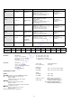
Hier finden Sie das Service-Manual für die Modelle KV-29FS60A bis KV-29FS60U und KV-32FS60A bis KV-32FS60E. SERVICE MANUAL CHASSIS NO. RM-891 Italian SCC-Q12E-A RM-891 French SCC-Q13E-A RM-891 AEP SCC-Q11E-A RM-891 Spanish SCC-Q14E-A RM-891 OIRT SCC-Q16G-A RM-891 OIRT SCC-Q16H-A RM-891 UK SCC-Q15D-A MODEL COMMANDER KV-32FS60A KV-32FS60B KV-32FS60D KV-32FS60E DEST CHASSIS NO.
Italian Television System Stereo System B/G/H,D/K GERMAN Stereo French B/G/H, D/K,L,I GERMAN/NICAM Stereo AEP B/G/H, D/K GERMAN Stereo Spanish B/G/H, D/K GERMAN/NICAM Stereo KV-29FS60K GERMAN/NICAM Stereo B/G/H, D/K OIRT Channel Coverage ITALIA VHF : A-H2 (C) UHF : 21-69 PAL B/G/H VHF : E2-E12 UHF : E21-E69 CABLE TV (1) : S1-S41 CABLE TV (2) : S01-S05,M1-M10,U1-U10 DK VHF : R01-R12 UHF : R21-R69 PAL, SECAM NTSC4.
[RM-891] Remote control system Power requirements Dimensions Weight Infrared control 3V dc 2 batteries IEC designation R6 (size AA) Approx 210x56x24mm (w/h/d) Approx 110g (Not including battery) Design and specifications are subject to change without notice.
21 pin connector Pin No 1 2 4 Signal 2 2 3 S3 G Signal level Audio output B (right) Standard level : 0.5V rms Output impedence : Less than 1kohm* 2 Audio output B (right) Standard level : 0.5V rms Output impedence : More than 10kohm* 3 Audio output A (left) Standard level : 0.5V rms Output impedence : Less than 1kohm* 4 Ground (audio) 5 Ground (blue) 6 Audio input A (left) Standard level : 0.5V rms Output impedence : More than 10kohm* 7 Blue input 0.
AE-5 SELF DIAGNOSTIC SOFTWARE The identification of errors within the AE-5 chassis is triggered in one of two ways :- 1: Busy or 2: Device failure to respond to IIC. In the event of one of these situations arising the software will first try to release the bus if busy (Failure to do so will report with continuous flashing LED) and then communicate with each device in turn to establish if a device is faulty.
ERROR DETECTION MONITOR Device acknowledge is used to check IIC errors. Device acknowledge is checked by sending an IIC start sequence during CRT power on. Each device is checked three times, if there is no acknowledge after every attempt, it will be regarded as an error. There are three steps to check errors 1. IIC line 0 If all devices except the NVM have errors, IIC line 0 error is displayed 2. Board check If all devices mounted on one board have errors, board error is displayed 3.
2. ERROR READER DISPLAY The error reader display is connected to the service connector to read actual error codes. The part number for the error reader display is S-188-900-10. Once an error has been detected it will then be displayed on the two digit error reader. The errors displayed refer to the following table : Send Data to Error Reader Error Code Data high Data Low Error type 00 00h - f0h no device 00 01h f0h 01h IIC 0 line 00 02h f0h 02h IIC 1 line Function Gen.
TABLE OF CONTENTS Section Title Page Warning and Caution Self-Diagnostic Function Section Title 5-1. 1. GENERAL Overview Installation Advanced Operations Teletext .....................9 .....................10 .....................11 .....................16 5-2. 5-3. 2. DISASSEMBLY .....................17 .....................17 .....................17 .....................17 .....................18 .....................18 .....................18 .....................19 .
SECTION 1 GENERAL TV-set – front and top Overview Symbol Description See page 1 TVI/u TV: standby mode on/off . . . . . . . . . . . . . . . . . . . . . . . . . . . . . . . . . . . . . 32 2 + ; TV: on-screen display . . . . . . . . . . . . . . . . . . . . . . . . . . . . . . . . . . . . . . . . 32 Teletext: index page . . . . . . . . . . . . . . . . . . . . . . . . . . . . . . . . . . . . . . . . . . 42 3 R Selecting of input source . . . . . . . . . . . . . . . . . . . . . . . . . . . . . . . .
Step 2 Basic Presetting Installation B Connecting the TV Set 1 2a 2b A The Menu System Connect the TV set to the mains socket (220-240 V. AC, 50 Hz). Connect a conventional aerial cable to the socket marked ˘ M on the rear of the TV set or Connect your Satellite Receiver to one of the Scart connectors J K L of the TV set. Your TV uses an on-screen menu system to guide you through the operations.
Step 3 Basic TV operation Advanced Operation This section explains the most important functions for the daily use of your TV set. When using the control panel on the top of the TV set, first press CONTROL I, then F, G or H. • Press U E on the TV set. To save energy, we recommend to switch off the TV completely when set is not in use. Switching off temporarily (Standby mode) • Press TV I/ u 1. TV is now in standby mode. Indicator u D lights up. After 15 min.
Advanced Presetting Advanced Presetting Selecting your NexTView Provider* Captioning a Station Name *depending on availability of service During presetting the channels are usually labelled automatically. You can, however, individually name a channel or a video input source. using $. Push to ”. 1 Press MENU. Select the symbol 2 Select Installation using $. Push to ” to enter. Select Manual Programme Preset using $. Push to ” to enter.
Advanced Presetting Advanced Presetting Adjusting the Picture Geometry for an RGB Source Inputting Your Personal ID by pressing … repeatedly. O H S ze O Press MENU. Select the symbol Select Installation using $. Push to ” to enter. Select RGB Set Up using $. Push to ” to enter. 4 Select H Centre by pushing to ”. Adjust the centre of the picture (range from -10 to +10) using 4 or $. Store by pressing OK. 5 Select H Size using $. Push to ” to enter.
Advanced TV operation Advanced TV operation Sound Control (continued) Adjusting Picture and Sound Item Picture and sound are adjusted at the factory. You can however, adjust them individually. Press MENU. Select the symbol for Picture or for Sound using 4 or $. Push to ” to enter. The menu Picture or Sound Control is displayed. 2 Select the desired item using 4 or $. Push to ” to enter. 3 Adjust the selected item using 4, $, ” and “. Press OK to store.
Advanced TV operation Advanced TV operation Using Screen Mode Using the Features Menu Press MENU. Select the symbol 2 Select the desired menu item using $. Push z to enter. 3 Select the desired setting using 4 or $. 4 Store by pressing OK. 5 When Auto Format in the Features menu is preset to »On« and a format signal is being transmitted, the TV set automatically selects the detected screen format. Screen mode, however, lets you select the screen format of your choice.
Teletext Teletext Most TV channels broadcast information via teletext. The index page of the teletext service (usually page 100) gives you information on how to use the service. Using the Teletext Menu Make sure to use a TV channel with a strong signal, otherwise there may be Teletext errors. This TV set has a menu-guided teletext system. When teletext is switched on you can use the joystick buttons to operate the teletext menu.
SECTION 2 DISASSEMBLY 2-1. REAR COVER REMOVAL 2-2. CHASSIS ASSY REMOVAL .d e 2 Rear Cover .E LE K O 1 6 Screws BTV 4x16 CAUTION: Take care not to damage the C Board when removing or refitting the rear cover. 2-4. U BOARD REMOVAL w w w 2-3. SERVICE POSITION 1 Push the claw in the direction of the arrow and remove. 2 Pull the Board in the direction of the arrow and remove.
2-5. J BOARD REMOVAL 2-6. J SHIELD REMOVAL 1 Push the claw in the direction of the arrow and remove. 1 Push the claw in the direction of the arrow and remove. .E LE K O .d e 3 Remove the shield in the direction of the arrow. 2 Pull the Board in the direction of the arrow and remove. NOTE w w 2-7. B1 BOARD REMOVAL w All other boards are removed in a similar manner to those shown 18 2 Push the claw in the direction of the arrow and remove.
2-8. PICTURE TUBE REMOVAL 7 DGC holder Degaussing coils 8 Spring tension 9 C board 3 2 Chassis assy .d e VM board 4 O Neck assy 5 .E LE K Deflection yolk 6 Anode cap 1 10 Four PT screws w Picture tube 11 w REMOVAL OF ANODE-CAP w • Cushion Note : Short circuit the an de of the picture tube and the anode cap to the metal chassis, CRT shield or carbon paint on the CRT, after removing the anode. * REMOVING PROCEDURES.
£ REMOVAL AND REPLACEMENT OF THE MAIN-BRACKET BOTTOM PLATES. (2) REFITTING THE PLATES Because the plates differ in size it is important that the correct plates are refitted in their original location. e REMOVING THE PLATES In the event of servicing being required to the solder side of the D Board printed wiring board, the bottom plates fitted to the main chassis bracket require to be removed. This is performed by cutting the gates with a sharp wire cutter at the locations indicated by arrows.
SECTION 3 SET-UP ADJUSTMENTS • • • Carry out the following adjustments in this order: When complete readjustment is necessary or a new picture tube is installed, carry out the following adjustments. Unless there are specific instructions to the contrary, carry out these adjustments with the rated power supply. Unless there are specific instructions to the contrary, set the controls and switches to the following settings: Contrast ............... normal Brightness ............... normal 3-1. 3-2. 3-3.
Center dot GREEN RED BLUE Fig.3-4 H.STAT convergence control H.STAT VR on mount side RV5376 Screen (G2) O Purity control corrects this area. .d e Disk magnets or rotatable disk magnets correct these areas (a-d). V.STAT vertical static magnet .E LE K H.STAT convergence • (Open) (Close) w w w Deflection yoke positioning corrects these areas If the horizontal dots are unable to coincide with the variable range of the H.STAT convergence, adjust together with the V.
By rotating the V.STAT magnet clockwise, the red, green and blue dots move in the direction indicated below. B R 7. By opening or closing the V.STAT magnet, the red, green and blue dots move in the direction indicated below. B R G G R B If the blue dot does not coincide with the red and green points correct the points by using the BMC [Hexapole] magnet. .E LE K Note : 5. Correction for HMC [horizontal mis-convergence] and VMC [vertical mis-convergence] by using the BMC [Hexapole] magnet. a).
Layout of each control 3-3. FOCUS 1. 2. 3. Purity magnet BMC (Hexaploe) magnet V STAT convergence magnet .d e Y-splitting axis correction magnet O Fig 3-5 If you are unable to adjust the corner convergence properly, this can be corrected with the use of permalloys. .E LE K Note : Receive a television broadcast signal. Normalize the picture setting. Adjust the focus control located on the flyback transformer to obtain the best focus at the centre of the screen.
White balance adjustment for TV mode Min Max Data 1 R-on ON OFF ON ON 2 G-on ON OFF ON ON 3 B-on ON OFF ON ON 4 D-col OFF OFF ON ON 5 Color-axis 2 0 3 2 6 Contrast 63 0 63 63 7 Limit-Luv 3 0 3 3 8 Hue 31 0 63 31 9 Colour 31 0 63 28 CTI -Level 2 0 3 2 10 11 12 13 .d e Def Brightness 31 0 63 31 Gamma 2 0 3 2 Sharpnes 31 0 63 44 LTI-Level 0 0 3 0 40 O 12. Descr.
SECTION 4 CIRCUIT ADJUSTMENTS 4-1. ELECTRICAL ADJUSTMENTS Service adjustments to this model can be performed using the supplied Remote Commander RM-891. HOW TO ENTER INTO SERVICE MODE 1. Turn on the main power switch of the set while pressing PROG + (plus) and PROG - (minus) buttons on the top panel. – PROGR + – + O "TT" will appear in the upper right corner of the screen. Press the ‘MENU’ button twice on the remote commander to obtain the service menu on the s reen. .E LE K 2. 3. .
Backend Model Setting KV-29FX60A/D/E Descr.
Deflection Feature setting No 1 Descr. Min Max Data No Descr. Def Min Max Data PIP OFF ON ON 1 V-Size 31 0 63 34 2 V-Position 31 0 63 21 3 V-Comp 1 0 3 1 4 V-Linear 7 0 15 7 5 S-Corr 7 0 15 8 6 H-Size 31 0 63 29 7 EW-DC OFF OFF ON OFF 8 Pin-Amp 31 0 63 36 Fig.
Feature Low-End Feature Low-End(Cont.) No Descr. Def Min Max Data No Descr. Def Min Max Data 1 F.S.F.M OFF OFF ON OFF 41 Hbdasta 223 0 255 223 2 G-Mode OFF OFF ON OFF 42 Hbdasto 222 0 255 222 3 Picture Pos 0 0 3 0 43 Hresta 38 0 255 38 4 Comp Mode OFF OFF ON OFF 44 Hresto 202 0 255 202 5 CompSW OFF OFF ON OFF 45 Hblndsta 31 0 255 31 6 Acqu.
PIP Feature Low-End (Cont.) No 81 Descr. Def Dcti Thres 0 Min 0 Max 15 Data No Descr.
Sound No Descr. Special Adjustment Def Min Max Data No 1 Ref.Level 40 0 20 40 1 RGB Level 2 Auto-gain ON OFF ON ON 2 3 Ana-in 0 0 1 0 3 4 Corr-mute ON OFF ON ON 4 RGB Patgain 5 Clock out ON OFF ON ON 5 RGB H-position 6 AM-gain ON OFF ON ON 6 Extra Fw Descr.
1. 2. DEFLECTION SYSTEM ADJUSTMENT V SIZE Enter into the service mode and select ‘Deflection ’. The ‘Deflect ’ adjustment menu will be displayed. Select and adjust each item to obtain the optimum image. V POS 4-2.VOLUME ELECTRICAL ADJUSTMENTS V LIN Sub Colour Adjustment Input a PAL colour bar signal. Connect an oscilloscope to CN5400 pin 5 on the C board. Enter into the ‘SERVICE MODE’. Choose ‘Backend’. Adjust Sub Colour data so that the right sides of the waveforms are of equal height. .E LE K O .
4-3. TEST MODE 2: Is available by pressing ‘TEST’ button twice, OSD ‘TT’ appears. The functions described below are available by pressing the two numbers. To release the Test mode 2, press 0, 10, 20 ... twice or switch the TV set into Stand-by Mode. Pressing the two Local Control buttons ( + and - ) during Power ON will also switch into ‘TT’ mode. In ‘TT’ mode, it is possible to remove the Menu from the screen by pressing the Speaker Off button once.
e .d 5-1 BLOCK DIAGRAMS (1) CN8 0 (2 2) V S B B Y Y V 0 V D 09 V V V B 0 V 9 V B 0 V V S S V 820 S SS V V S 0 0 B S SS V S 0 0 S Y B S V V S .
e D( OWER SU AND DE .
e SWCK IC2302 V MAIN IN A 7 U MAIN IN A 6 MA N IN 2 0 BAND ASS I ER IC2304 9 0 82 V D7 3 7 0 83 V D6 D5 2 3 0 72 V D4 2 D3 2 C D2 2 D 2 D0 2 UV3 2 UV2 2 UV UV0 (7) (7) (6) (6) (5) (5) (4) (4) (3) (3) (2) (2) ( ) ( ) (0) (0) U( ) U( ) U (0) U (0) V( ) V( ) V (0) V (0) 7 7 O7 2 8 6 O6 2 9 5 O5 2 0 4 O4 2 3 2 2 3 O2 2 I O 0 4 2 O3 2 UO UI 0 UO0 2 3 VI VO 4 V 0 VO0 7 2 O0 2 UI 2 7) H 7) H 6) H 6) H 5) H 5) 4) H 4) H 3) H
e CN6 0 ( 2) U 3 6 A( U 350 (SUB- UNER) S GNA AND AUDIO AM ) SC S SDA BU ER Q 328 Q 329 QSS C BS AC ON O QSS O AUD O SURRO ND AUD O CEN U OU HEAD HONE E MU E W Q 08 4 HE D HONE R GH HE D HONE E N OU AV3 E 7 AV3 AV3 MU E OU C MU E S B MU E IN U IC 26 AUDIO AM RIGH N U AV3 R GH OU 6 3 C 6 AUD O AM I ER CEN ER AND SURROUND I IER CN AUD O RESE H U E UB IN 9 V U E UB IN 9 V UB IN 20 U SUB N CN 02 9 0 GREEN 0 X OU EX RA RABO A BACK D NAM C 7 O D BOARD CN6 2
w w LE K .E w O .
LE K .E w w w O .
LE K .E w w w O .
.d e LE KO .
LE K .E w w w O .
LE K .E w w w O .
.d e O LE K .
LE K .E w w w O .
LE K .E w w w O .
KO LE .E w w w .
KO LE .E w w w .
LE K .E w w w O .
e .d KO .
Waveforms A Board 1 2 1.0 Vp-p (H) 3 2.0 Vp-p (H) 2.0 Vp-p (H) Waveforms D Board 2 40 mVp-p (H) 6 7 180 Vp-p (H) 20 mVp-p (H) 12 0.1 Vp-p (H) 14 .E LE K 2 0.4 Vp-p (H) 5 3 1.2 Vp-p (H) 0 2 Vp-p (H 6 0 2 Vp-p (H) 4 1.0 Vp-p (H) 7 1.0 Vp-p (H) w w 1 2 Vp-p (H) forms C Board w Wa 1 124.0 Vp-p (H) 180 V p (H) 20 Vp-p (H) 0.3 Vp-p (H) Waveforms J1(1/2) Board 1 1.1 KVp-p (H) 2.0 Vp-p (H) 13 2.0 Vp-p (V) 10 9 8 O 11 1.1 KVp-p (H) 2.
5-4 SEMICONDUCTORS M27C800-100K1 KA78R05TU KA78R09TU KA78R33TU BA7046F BA7046F-T1 LM393PS-E20 MB3793-42NF MB3793-42NF-ER NJM2240M NJM2240M(TE2) NJM3404AD 6 1 44 TC55257DFTL-70V-EL 40 7 39 17 1 2 3 4 1 : : : : 1 2 3 4 V IN V OUT GND ON/OFF CONTROL CXA1855Q-T6 4 3 48 13 1 1 2 6 5 SBX1981-51 3 CXA1875AM-T4 HE4094BT MC14052BDR2 MC74F157ADR2 SN74LS221D 74HCT4046AD/S470 17 16 1 ( TOP VIEW ) TDA9320H-N1-518 w 23 51 33 34 22 52 32 44 12 64 20 UT 1 w GND 32 SDA9361 33 I
U2860B-BFPG3 74LVC08D IMZ1A-T109 4 14 8 3 DAN202K DAN202K-T-146 2SC2500-B 2SC2551-O 2SC2551O-TPE2 5 3 6 1 2 1 2 6 5 4 7 1 ( TOP VIEW ) 2 3 BC546B BC556B 1 2 3 1 E C B IRF614 IRF620 DAP202K DAP202K-T-146 2SC2688-LK 2SC3840K 3 1 G .d e S D B E O C BF199 BF199-AMMO E DTC144EK DTC144EK-T146 2SA1037K-T-146-R 2SA1162-G 2SC2412K-QR 2SC2412K-T-1 6-R B C .
D4SB60L D4SB60L-F RBA-402L ESAC39M-06C ESAC39M-06CF38 UF4005PKG23 ANODE CATHODE 2 1 3 2 O MA3033-L MA3033L-TX MA3056M-TX MA3062M-TX MA3030-H-(TX) 3 .E LE K MTZJ-T-77-5.6B MTZJ-T-77-6.8 MTZJ-T-77-7.5B MTZJ-T-77-9.1 MTZJ-33C RD5.6ESB2 RD9.1ESB2 PGKE200AG23 1SS119-25 1SS119-25TD ERA38-06TP1 ERA82-004TP1 GP08DPKG23 MTZJ-T-77-12 MTZJ-T-77-15 MTZJ-T-77-2.2B MTZJ-T-77-22 MTZJ-T-77-33C MTZJ-T-77-3.6B MTZJ-T-77-4.7B 3 .
5-5. IC BLOCK DIAGRAMS D BOARD IC6700 STV 9379 2 6 J BOARD IC8101 TDA2822D 3 2 FLYBACK GENERATOR - 1 POWER AMPLIFIER 1 6 5 3 5 + 7 7 8 THERMAL PROTECTION 4 .d e 4 56 48 51 50 54 49 52 45 46 O E BOARD IC4301 CXA2100Q-TL 47 40 41 H SYNC SEP 53 S SEP VIDEO SW 55 SUB CONT 57 SHARP NESS DL TRAP DC TRAN CLP D PIC ACC DET Y/C w 2 PAL/ NTSC PAL ID 42 H.DRIVE fsc ID YS SW MIX 60 DEM A S 62 61 4 w 43 VCO w I REF 1 10 30 34 35 WIDE Sawtooth Gen.
SECTION 6 EXPLODED VIEWS NOTE : • • Items with no part number and no description are not stocked because they are seldom required for routine service. The construction parts of an assembled part are indicated with a collation number in the remarks column. • Items marked “ * “ are not stocked since they are seldom required for routine service. Some delay should be anticipated when ordering these items.
The components identified by shading and marked are critical for safety Replace only with the part number specified. 35 36 37 130 DESCRIPTION REMARK SCREW (4X16), (+) BV TAPPING SPEAKER (4.
6-2. PICTURE TUBE 70 76 69 77 68 78 79 75 72 74 71 .d e 80 73 .E LE K O 51 61 64 69 68 66 67 65 63 62 57 58 52 61 60 55 52 56 w 59 w 54 w 53 REF. NO. PART.
The components identified by shading and marked are critical for safety Replace only with the part number specified. DESCRIPTION 75 4-036-188-01 4-203-043-01 4-308-870-00 1-452-094-00 1-425-032-00 X-4387-214-1 3-701-007-00 SCREW, SELF TAPPING (KV-29FS60) SCREW (PT) (KV-32FS60) CLIP, LEAD WIRE MAGNET, ROTATABLE DISK; 15MM MAGNET, DISK; 10MM PERMALLOY ASSY, CORRECTION BAND, BINDING 76 77 78 79 80 .
SECTION 7 ELECTRICAL PARTS LIST • • • • • • Items marked “ * “ are not stocked since they are seldom required for routine service. Some delay should be anticipated when ordering these items. All variable and adjustable resistors have characteristic curve B, unless otherwise noted. RESISTORS All resistors are in ohms. F : nonflammable. When indicating parts by reference number, please include the board name.
B1 DESCRIPTION REMARK C2388 C2389 C2390 C2391 C2704 1-136-479-11 1-163-085-00 1-163-243-11 1-163-243-11 1-126-934-11 C2705 1-164-004-11 CERAMIC CHIP 0.1MF FILM 0.001MF CERAMIC CHIP 2PF CERAMIC CHIP 47PF CERAMIC CHIP 47PF ELECT 220MF 1% 0.
B1 REMARK REF. NO. PART.NO 1-216-057-00 1-216-057-00 1-216-057-00 1-216-057-00 1-216-065-91 RES,CHIP RES,CHIP RES,CHIP RES,CHIP RES,CHIP 2.2K 2.2K 2.2K 2.2K 4.
BP C331 C332 C333 C334 C335 1-163-038-91 1-126-964-11 1-163-038-91 1-126-964-11 1-126-964-11 CERAMIC CHIP 0.1MF ELECT 10MF CERAMIC CHIP 0.1MF ELECT 10MF ELECT 10MF C336 C337 C338 C339 C340 1-126-964-11 1-126-964-11 1-126-964-11 1-126-964-11 1-126-964-11 ELECT ELECT ELECT ELECT ELECT REF. NO. PART.NO 20% 20% 25V 50V 25V 50V 50V C384 C385 C386 C387 C388 1-126-964-11 1-163-231-11 1-126-964-11 1-163-038-91 1-163-038-91 ELECT 10MF CERAMIC CHIP 15PF ELECT 10MF CERAMIC CHIP 0.1MF CERAMIC CHIP 0.
BP DESCRIPTION IC309 IC311 IC312 8-759-295-09 IC TLC2932IPW 8-759-062-66 IC TC7S66F 8-759-062-66 IC TC7S66F REMARK < COIL > 1-412-029-11 1-410-435-21 1-410-435-21 1-412-029-11 1-410-435-21 INDUCTOR CHIP 10UH INDUCTOR 220UH INDUCTOR 220UH INDUCTOR CHIP 10UH INDUCTOR 220UH L305 L306 L307 L308 L309 1-410-435-21 1-412-029-11 1-412-029-11 1-412-029-11 1-412-029-11 INDUCTOR INDUCTOR INDUCTOR INDUCTOR INDUCTOR CHIP CHIP CHIP CHIP 220UH 10UH 10UH 10UH 10UH L311 L312 L313 L314 L315 1-412-029-11 1-412-029
PART.NO DESCRIPTION REMARK PART.NO R344 R345 R346 R347 R351 1-216-057-00 1-216-623-11 1-216-623-11 1-216-623-11 1-216-049-91 RES,CHIP METAL CHIP METAL CHIP METAL CHIP RES,CHIP 2.2K 68 68 68 1K 5% 0.50% 0.50% 0.50% 5% 1/10W 1/10W 1/10W 1/10W 1/10W R406 R407 R408 R409 R410 1-216-017-91 1-216-025-91 1-216-017-91 1-216-057-00 1-216-057-00 RES,CHIP RES,CHIP RES,CHIP RES,CHIP RES,CHIP 47 100 47 2.2K 2.
The components identified by shading and marked are critical for safety Replace only with the part number specified. BP PART.NO DESCRIPTION REMARK R464 R465 R466 R468 R469 1-216-638-11 1-216-636-11 1-216-049-91 1-216-017-91 1-216-017-91 METAL CHIP METAL CHIP RES,CHIP RES,CHIP RES,CHIP 330 240 1K 47 47 0.50% 0.
A REF. NO. PART.NO C1132 C1133 C1134 C1135 C1136 1-163-021-91 1-164-004-11 1-126-961-11 1-164-004-11 1-164-004-11 CERAMIC CERAMIC ELECT CERAMIC CERAMIC CHIP 0.01MF CHIP 0.1MF 2.2MF CHIP 0.1MF CHIP 0.1MF 10% 10% 20% 10% 10% 50V 25V 50V 25V 25V C1614 C1615 C1617 1-164-004-11 CERAMIC CHIP 0.1MF 1-164-004-11 CERAMIC CHIP 0.1MF 1-164-004-11 CERAMIC CHIP 0.1MF C1137 C1138 C1139 C1140 C1151 1-126-953-11 1-126-953-11 1-104-329-11 1-111-216-91 1-162-568-11 ELECT 2200MF ELECT 2200MF CERAMIC CHIP 0.
A REF. NO. PART.NO DESCRIPTION REMARK IC1603 IC1604 IC1605 8-759-295-82 IC L78L08ACZ-AP 8-759-544-13 IC KA78R09TU 8-759-544-11 IC KA78R33TU < COIL > REF. NO. PART.NO DESCRIPTION REMARK R1176 R1177 R1178 R1179 R1180 1-216-063-91 1-216-063-91 1-216-357-00 1-216-357-00 1-216-081-00 RES,CHIP RES,CHIP METAL OXIDE METAL OXIDE RES,CHIP 3.9K 3.9K 4.7 4.7 22K 5% 5% 5% 5% 5% 1/10W 1/10W 1W F 1W F 1/10W 1-416-966-11 1-414-158-11 1-535-143-61 1-416-966-11 1-414-158-11 CHOKE, COIL 30uH INDUCTOR 2.
M DESCRIPTION REF. NO. PART.
M PART.NO DESCRIPTION D9103 D9104 D9105 D9107 D9108 8-719-988-62 8-719-056-83 8-719-914-43 8-719-025-31 8-719-914-44 D9109 D9110 D9111 8-719-105-91 DIODE RD5.6M-B2 8-719-914-43 DIODE DAN202K 8-719-105-91 DIODE RD5.6M-B2 DIODE DIODE DIODE DIODE DIODE REMARK 1SS355 UDZ-TE-17-6.8B DAN202K 02CZ5.
M C REMARK R9186 R9187 R9188 R9189 R9190 1-216-025-91 1-216-065-91 1-216-025-91 1-216-025-91 1-216-025-91 RES,CHIP RES,CHIP RES,CHIP RES,CHIP RES,CHIP 100 4.
The components identified by shading and marked are critical for safety Replace only with the part number specified. PART.NO DESCRIPTION D5378 D5379 D5380 D5381 8-719-921-88 8-719-982-96 8-719-982-96 8-719-031-34 DIODE DIODE DIODE DIODE REMARK MTZJ-13B MTZJ-T-77-2.2A MTZJ-T-77-2.
E C4338 C4340 C4342 C4343 C4344 1-164-004-11 1-126-967-11 1-163-021-91 1-164-004-11 1-163-809-11 CERAMIC ELECT CERAMIC CERAMIC CERAMIC CHIP 0.1MF 47MF CHIP 0.01MF CHIP 0.1MF CHIP 0.047MF C4345 C4346 C4347 C4348 C4349 1-126-967-11 1-164-004-11 1-164-004-11 1-164-004-11 1-164-004-11 ELECT CERAMIC CERAMIC CERAMIC CERAMIC CHIP CHIP CHIP CHIP C4350 C4351 C4352 C4353 C4354 1-164-004-11 1-163-009-11 1-126-967-11 1-107-823-11 1-107-823-11 CERAMIC CERAMIC ELECT CERAMIC CERAMIC CHIP 0.1MF CHIP 0.
E REMARK 1-216-025-91 1-216-025-91 1-216-677-11 1-216-683-11 1-216-025-91 RES,CHIP RES,CHIP METAL CHIP METAL CHIP RES,CHIP 100 100 12K 22K 100 5% 5% 0.50% 0.50% 5% 1/10W 1/10W 1/10W 1/10W 1/10W R4348 R4350 R4354 R4358 R4359 1-216-025-91 1-216-025-91 1-216-675-11 1-216-071-00 1-216-041-00 RES,CHIP RES,CHIP METAL CHIP RES,CHIP RES,CHIP 100 100 10K 8.2K 470 5% 5% 0.
D1 PART.NO DESCRIPTION REMARK C6121 C6122 C6125 C6126 C6127 1-126-964-11 1-126-967-11 1-163-017-00 1-163-809-11 1-163-021-91 C6128 C6129 1-163-017-00 CERAMIC CHIP 0.0047MF 10% 50V 1-115-339-11 CERAMIC CHIP 0.1MF 10% 50V (KV-29FS60A/29FS60B/29FS60D/29FS60E/ 29FS60K/29FS60R/29FS60U) 1-164-336-11 CERAMIC CHIP 0.
The components identified by shading and marked are critical for safety Replace only with the part number specified. PART.NO D6355 DESCRIPTION REF. NO. PART.NO D6358 D6359 8-719-914-43 DIODE DAN202K (KV-32FS60A/32FS60B/32FS60D/32FS60E) 1-216-667-11 METAL CHIP 4.7K 0.
D1 REF. NO. PART.NO 1-216-679-11 METAL CHIP 15K 0.50% 1/10W (KV-29FS60A/29FS60B/29FS60D/29FS60E/ 29FS60K/29FS60R/29FS60U) 1-216-683-11 METAL CHIP 22K 0.50% 1/10W (KV-32FS60A/32FS60B/32FS60D/32FS60E) R6142 1-216-672-11 METAL CHIP 7.5K 0.50% 1/10W (KV-29FS60A/29FS60B/29FS60D/29FS60E/ 29FS60K/29FS60R/29FS60U) 1-216-659-11 METAL CHIP 2.2K 0.
D1 R6180 R6182 R6183 R6186 1-216-057-00 1-216-089-91 1-216-057-00 1-216-663-11 R6187 R6189 DESCRIPTION REMARK RES,CHIP 2.2K 5% 1/10W RES,CHIP 47K 5% 1/10W RES,CHIP 2.2K 5% 1/10W METAL CHIP 3.3K 0.50% 1/10W (KV-29FS60A/29FS60B/29FS60D/29FS60E/ 29FS60K/29FS60R/29FS60U) 1-216-049-91 METAL CHIP 1K 5% 1/10W (KV-32FS60A/32FS60B/32FS60D/32FS60E) 1-216-065-91 RES,CHIP 4.
D1 R6284 DESCRIPTION REF. NO. PART.NO 1-216-113-00 RES,CHIP 470K 5% 1/10W (KV-29FS60A/29FS60B/29FS60D/29FS60E/ 29FS60K/29FS60R/29FS60U) 1-216-109-00 RES,CHIP 330K 5% 1/10W (KV-32FS60A/32FS60B/32FS60D/32FS60E) R6372 R6373 R6374 R6375 R6377 1-216-033-00 1-216-681-11 1-216-689-11 1-216-041-00 1-216-689-11 RES,CHIP METAL CHIP METAL CHIP RES,CHIP METAL CHIP 220 18K 39K 470 39K 5% 0.50% 0.50% 5% 0.50% R6285 R6286 1-216-057-00 RES,CHIP 2.
The components identified by shading and marked are critical for safety Replace only with the part number specified. REMARK REF. NO. PART.NO R6432 R6433 R6437 1-216-113-00 RES,CHIP 470K 5% 1/10W (KV-32FS60A/32FS60B/32FS60D/32FS60E) 1-216-057-00 RES,CHIP 2.2K 5% 1/10W 1-216-073-00 RES,CHIP 10K 5% 1/10W 1-249-422-11 CARBON 2.
The components identified by shading and marked are critical for safety Replace only with the part number specified. D 1-129-702-00 1-106-220-00 1-102-129-00 1-130-785-11 1-102-228-00 FILM MYLAR CERAMIC MYLAR CERAMIC 0.001MF 0.1MF 0.01MF 0.
The components identified by shading and marked are critical for safety Replace only with the part number specified. D6655 D6656 D6658 D6659 D6676 8-719-979-64 8-719-510-64 8-719-068-00 8-719-510-64 8-719-991-33 DIODE DIODE DIODE DIODE DIODE D6677 D6678 D6679 D6700 D6701 8-719-921-40 8-719-921-40 8-719-991-33 8-719-908-03 8-719-110-41 D6803 D6804 D6805 D6806 D6807 REF. NO. PART.
The components identified by shading and marked are critical for safety Replace only with the part number specified. D DESCRIPTION REMARK Q6810 Q6851 8-729-026-41 TRANSISTOR 2SA933AS-QRT 8-729-043-95 TRANSISTOR 2SC3840(3) < RESISTOR > £ 1-202-968-11 1-249-430-11 1-249-421-11 1-249-417-11 £ 1-202-968-11 CEMENTED CARBON CARBON CARBON CEMENTED 1.2 12K 2.2K 1K 1.
The components identified by shading and marked are critical for safety Replace only with the part number specified. DESCRIPTION R6817 R6818 R6819 R6831 R6832 1-216-361-00 1-247-807-31 1-247-807-31 1-260-124-11 1-216-434-11 R6833 R6834 R6835 R6836 R6837 1-202-972-61 1-249-377-11 1-249-377-11 1-249-431-11 1-215-919-11 METAL OXIDE CARBON CARBON CARBON METAL OXIDE REMARK 0.22 100 100 120K 1.8K 5% 5% 5% 5% 5% 2W F 1/4W 1/4W 1/2W 1W F FUSIBLE 1 5% 1/4W F CARBON 0.47 5% 1/4W F CARBON 0.
PART.
U DESCRIPTION C7961 C7962 1-101-005-00 CERAMIC 1-101-005-00 CERAMIC REMARK 0.022MF 0.
J DESCRIPTION C8232 C8233 C8234 C8235 C8236 1-164-004-11 1-104-664-11 1-107-823-11 1-107-823-11 1-126-933-11 CERAMIC CHIP 0.1MF ELECT 47MF CERAMIC CHIP 0.47MF CERAMIC CHIP 0.47MF ELECT 100MF 10% 20% 10% 10% 20% 25V 16V 16V 16V 16V C8237 C8238 C8239 C8240 C8241 1-163-021-91 1-164-505-11 1-107-823-11 1-107-823-11 1-126-964-11 CERAMIC CERAMIC CERAMIC CERAMIC ELECT 10% 50V 16V 16V 16V 50V C8242 C8243 1-104-664-11 ELECT 47MF 1-110-501-11 CERAMIC CHIP 0.33MF CHIP CHIP CHIP CHIP REMARK 0.01MF 2.
J C8508 C8509 C8510 C8511 C8512 1-164-004-11 1-126-933-11 1-104-664-11 1-164-004-11 1-164-004-11 CERAMIC CHIP 0.1MF ELECT 100MF ELECT 47MF CERAMIC CHIP 0.1MF CERAMIC CHIP 0.1MF 10% 20% 20% 10% 10% 25V 16V 16V 25V 25V C8513 C8514 C8515 C8516 C8517 1-164-004-11 1-164-004-11 1-164-004-11 1-164-004-11 1-164-004-11 CERAMIC CERAMIC CERAMIC CERAMIC CERAMIC CHIP CHIP CHIP CHIP CHIP 0.1MF 0.1MF 0.1MF 0.1MF 0.
J DESCRIPTION D8914 D8915 D8922 D8923 8-719-158-49 8-719-158-49 8-719-056-84 8-719-978-04 DIODE DIODE DIODE DIODE REMARK RD12SB2 RD12SB2 UDZ-TE-17-7.5B DTZ-TT11-3.3B PART.
J DESCRIPTION REMARK Q8901 Q8903 8-729-620-06 TRANSISTOR 2SC3052-EF 8-729-620-06 TRANSISTOR 2SC3052-EF 1-216-025-91 1-216-025-91 1-216-295-91 1-216-089-91 1-216-089-91 RES,CHIP RES,CHIP SHORT RES,CHIP RES,CHIP 100 100 0 47K 47K 5% 5% 1/10W 1/10W 5% 5% 1/10W 1/10W R8105 R8106 R8107 R8108 R8109 1-216-057-00 1-216-081-00 1-216-081-00 1-216-057-00 1-249-389-11 RES,CHIP RES,CHIP RES,CHIP RES,CHIP CARBON 2.2K 22K 22K 2.2K 4.
DESCRIPTION REF. NO. PART.NO 1/10W R8346 1-216-295-91 SHORT 1/10W 1/10W 1/10W R8347 1-216-025-91 RES,CHIP R8348 1-216-295-91 SHORT R8349 1-216-121-91 RES,CHIP 1M R8350 1-216-073-00 RES,CHIP 10K R8351 R8352 1-216-073-00 RES,CHIP 1-216-089-91 RES,CHIP 1K 7K R8353 1-216-081-00 RES,CHI 2K R8354 R8355 R8356 R8400 R8402 O J REF. NO. PART.
J REMARK REF. NO. PART.NO R8433 R8434 R8450 R8451 R8453 1-216-073-00 1-216-073-00 1-216-089-91 1-216-073-00 1-216-089-91 RES,CHIP RES,CHIP RES,CHIP RES,CHIP RES,CHIP 10K 10K 47K 10K 47K 5% 5% 5% 5% 5% R8454 R8455 R8460 R8462 R8467 1-216-073-00 1-216-057-00 1-216-057-00 1-216-073-00 1-216-089-91 RES,CHIP RES,CHIP RES,CHIP RES,CHIP RES,CHIP 10K 2.2K 2.
The components identified by shading and marked are critical for safety Replace only with the part number specified. REF. NO. PART.NO R8951 R8952 R8953 R8954 R8955 1-216-033-00 1-216-113-00 1-216-039-00 1-216-057-00 1-216-039-00 RES,CHIP RES,CHIP RES,CHIP RES,CHIP RES,CHIP 220 470K 390 2.
The components identified by shading and marked are critical for safety Replace only with the part number specified. REF. NO. PART.NO DESCRIPTION REMARK REF. NO. PART.NO DESCRIPTION ACCESSORIES AND PACKAGING MATERIALS (KV-29FS60) *********************************** 1-765-654-11 CABLE,SPEAKER 4-204-589-41 MANUAL, INSTRUCTION (KV-29FS60A) (ITALIAN) 4-204-589-51 MANUAL, INSTRUCTION (KV-29FS60B) (FRENCH/GERMAN/ITALIAN/DUTCH) .