
Datasheet

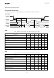


Table Of Contents
- Description
- Features
- Contents
- Package
- Structure
- Block Diagram
- Description of Functions
- Description of Operation
- Recommended operating conditions
- Absolute Maximum Ratings
- Temperature Condition
- Power Consumption
- Clocks
- Electrical Characteristics
- Serial peripheral interface (SPI)
- Quad SPI Flash Interface
- Inter-integrated circuit interface (I2C)
- Universal Asynchronous Receiver Transmitter (UART)
- Inter-integrated sound (I2S)
- Image Sensor Interface
- SD Host Interface
- eMMC Interface
- Universal serial bus (USB) Device
- RTC Signals
- Rise Edge Detection Mode
- Fall Edge Detection Mode
- ADC Analog Input Interface
- Serial wire debug (SWD)
- Notes on Handling
- Pin Configuration
- Pin Description
- Power Pins
- Ball Map
- Power On/Off sequence
- Application Circuits.
- Notice

CXD5602GG
26
Quad SPI Flash Interface
Quad SPI Flash Interface (SPI1) is available.
SPI1_SCK
(Output)
SPI1_IO[3:0]
(Output)
tSCK
tSLCH
tCHSH
SPI1_CS_X
(Output)
SPI1_IO[3:0]
(Input)
tOD
tSCKLtSCKH
tIS
tIH
(VDD_CORE=0.7V(LP)/1.0V(HP), VSS_DIG=0V reference, CL=15pF)
Parameter Symbol Min. Typ. Max. Units Notes
SPI1_SCK Period tSCK - 25.6 - ns 39MHz
SPI1_SCK Duty Ratio tSCKH / tSCK
(tSCKL/tSCK)
40 50 60 % -
SPI1_CS_X active setup time tSLCH 7 - - ns -
SPI1_CS_X active hold time tCHSH 5 - - ns -
SPI1_IO Output Delay Time tOD -10.36 - 12.86 ns -
SPI1_IO Input Setup Time tIS 0 - - ns -
SPI1_IO Input Hold Time tIH 15.36 - - ns -