
Datasheet


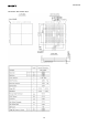

Table Of Contents
- Description
- Features
- Contents
- Package
- Structure
- Block Diagram
- Description of Functions
- Description of Operation
- Recommended operating conditions
- Absolute Maximum Ratings
- Temperature Condition
- Power Consumption
- Clocks
- Electrical Characteristics
- Serial peripheral interface (SPI)
- Quad SPI Flash Interface
- Inter-integrated circuit interface (I2C)
- Universal Asynchronous Receiver Transmitter (UART)
- Inter-integrated sound (I2S)
- Image Sensor Interface
- SD Host Interface
- eMMC Interface
- Universal serial bus (USB) Device
- RTC Signals
- Rise Edge Detection Mode
- Fall Edge Detection Mode
- ADC Analog Input Interface
- Serial wire debug (SWD)
- Notes on Handling
- Pin Configuration
- Pin Description
- Power Pins
- Ball Map
- Power On/Off sequence
- Application Circuits.
- Notice
CXD5602GG
48
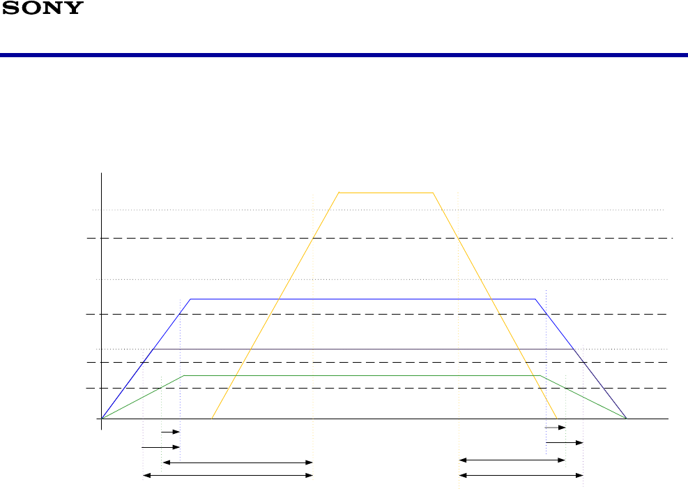
Power On/Off sequence
To a vo id oc cu rri ng re lia bi l i t y pro bl em a nd l o a d in g e xt e r n a l p owe r s u p p l y sy s te m, t ur ni ng o n t he I / O pow e r s u p pl y(1 .8 V
Domain) and then turning on the internal power supply(1.0/0.7V Domain) is recommended for power on. In addition, shutting
down the internal power supply (1.0/0.7V Domain) and then shutting down the I/O power supply (1.8V Domain) in the
reverse order of turning on is recommended for power off.
VDD
_
CORE
/
VDDA_
USB10
VDD
_
IO
_
DIG
/
VDDA
_
IO
_ANALOGs
/VDDA
_
USB18
VDDA_
ANALOGs
VDDA
_
USB
33
GND
0
.
7
V
1
.
0
V
3
.3
V
2
.
0
V
3
.
0V
1
.
8
V
VBUS ON
1
.0
V Domain x80
%
0.7V Domain x80%
3
.3
V Domain x
80%
1.
0
V
No constraints
1
.
8V Domain x
80%
VBUS OFF
sequence recomendation
No constraints
No constraints
No constraints
sequence recomendation
No constraints
No constraints