MDS-JE320 SERVICE MANUAL US Model Canadian Model AEP Model Model Name Using Similar Mechanism MDS-JE510 MD Mechanism Type MDM-3GC Optical Pick-up Type KMS-260A/J1NP SPECIFICATIONS MINIDISC DECK MICROFILM
CAUTION Laser component in this product is capable of emitting radiation exceeding the limit for Class 1. Danger of explosion if battery is incorrectly replaced. Replace only with the same or equivalent type recommended by the equipment manufacturer. Discard used batteries according to manufacture’s instructions. This appliance is classified as a CLASS 1 LASER product. The CLASS 1 LASER PRODUCT MARKING is located on the rear exterior. ADVARSEL! Lithiumbatteri - Eksplosionsfare ved fejlagtig håndtering.
SAFETY CHECK-OUT TABLE OF CONTENTS After correcting the original service problem, perform the following safety checks before releasing the set to the customer: Check the antenna terminals, metal trim, “metallized” knobs, screws, and all other exposed metal parts for AC leakage. Check leakage as described below. 1. SERVICING NOTE ..........................................................
[SELF-DIAGNOSIS FUNCTION] The self-diagnosis function consists of error codes for users which are displayed automatically when errors occur, and error codes which show the error history in the test mode during servicing.For detail on how to view error codes for users, refer to the following box in the instruction manual. Self-Diagnosis Function The deck has a self-diagnosis display.
SECTION 1 SERVICING NOTE JIG FOR CHECKING BD BOARD WAVEFORM The special jig (J-2501-124-A) is useful for checking the waveform of the BD board. The names of terminals and the checking items to be performed are shown as follows.
RETRY CAUSE DISPLAY MODE • In this test mode, the causes for retry of the unit during recording can be displayed on the fluorescent display tube. This is useful for locating the faulty part of the unit. • The data amount stored in DRAM, number of retries, and retry cause are displayed. Each is displayed in hexadecimal number. • The display of the DRAM data amount enables data reading, accumulation, ejection, and writing to be performed smoothly. If writing is not smooth, data may decrease considerably.
Reading the Retry Cause Display Higher Bits Hexadecimal 8 Bit Binary 4 2 1 Lower Bits 8 4 2 1 b7 b6 b5 b4 b3 b2 b1 b0 Hexa- Cause of Retry decimal Occurring conditions 0 0 0 0 0 0 0 0 00 Spindle is slow When spindle rotation is detected as slow 0 0 0 0 0 0 0 1 01 (Not used) (Not used) 0 0 0 0 0 0 1 0 02 ader5 0 0 0 0 0 1 0 0 04 Discontinuous address When ADIP address is not continuous (Not used) (Not used) When ADER was counted more than five times c
SECTION 2 GENERAL Location of Parts and Controls 1 2 3 4 !ª 1 1/u (Power) switch 2 Remote sensor 3 Display window 4 Disc compartment 5 AMS knob 6 0/) buttons 7 DISPLAY/CHAR button 8 INPUT switch 5 !• !¶ !§ 6 7 !∞ !¢ !£ 9 REC LEVEL knob !£ r REC (recording) button !¢ p (stop) button !∞ P (pause) button !§ · (play) button !¶ YES button !• EDIT/NO button !ª § EJECT button —8— 8 9
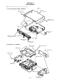
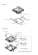
SECTION 3 DISASSEMBLY Note : Follow the disassembly procedure in the numerical order given. 4 Case 3-1. CASE AND FRONT PANEL ASSEMBLY 3 Screw (case 3 TP 2) 1 Two screws (Case 3 TP 2) 2 Two screws (Case 3 TP 2) 5 Ground terminal claw 6 Flat type wire (CN303) 9 Remove the front panel assembly releasing two claws. claw 8 Four screws (BVTP3×8) 7 Three screws (BVTP3×8) 3-2.
3-3. BD BOARD 2 Flat type wire (15 core) 4 OP relay flexible board 1 Flexible board (Over write head) 5 BD board 3 Screw (BVTT2×4) 3-4. SUB CHASSIS 1 Two step screws 2 Two step screws 3 Two insulators 4 Two insulators Part A NG Part A 5 Sub chassis Part A OK Take care so that the part A may be right position when installing.
3-5. SHUTTER ASSEMBLY 1 Stepper washer Shutter assembly Shaft (lid) 2 Shaft (shutter) 3 Shutter assembly Hole B Shaft (shutter) Hole A When installing, install the shaft (shutter) into the hole A as shown in the figure before installing the shaft (lid) into the hole B. 3-6. OVER WRITE HEAD 1 Precision screw (P1.
3-7. SLIDER COMPLETE ASSEMBLY 3 Set the shaft of Gear (LA) to be at the position in the figure. claw claw 45° 4 Remove the slider complete assembly in the direction of arrow with putting out of two claws. 1 Screw (M1.7×2) 2 Retainer (gear) • Note for Installation of Slider Complete Assembly Slider assembly Install the part A of lever (head up) to pass over the slider complete assembly. OK Part A NG Take care not to damage the detective switch.
SECTION 4 TEST MODE 4-1. PRECAUTIONS FOR USE OF TEST MODE 1 As loading related operations will be performed regardless of the test mode operations being performed, be sure to check that the disc is stopped before setting and removing it. Even if the §EJECT button is pressed while the disc is rotating during continuous playback, continuous recording, etc., the disc will not stop rotating. Therefore, it will be ejected while rotating.
4-5-1. Operating the Continuous Playback Mode 1. Entering the continuous playback mode 1 Set the disc in the unit. (Whichever recordable discs or discs for playback only are available.) 2 Rotate the AMS knob and display “CPLAY MODE”. 3 Press the YES button to change the display to “CPLAY MID”. 4 When access completes, the display changes to “C1 = AD = ”. Note : The numbers “ ” displayed show you error rates and ADER. 2.
4-6. FUNCTIONS OF OTHER BUTTONS Function Contents · Sets continuous playback when pressed in the STOP state. When pressed during continuous playback, the tracking servo turns ON/OFF. p Stops continuous playback and continuous recording. ) The sled moves to the outer circumference only when this is pressed. 0 The sled moves to the inner circumference only when this is pressed. r REC Turns recording ON/OFF when pressed during continuous playback. DISPLAY/ Switches the display when pressed.
SECTION 5 ELECTRICAL ADJUSTMENTS 5-1. PRECAUTIONS FOR CHECKING LASER DIODE EMISSINON To check the emission of the laser diode during adjustments, never view directly from the top as this may lose your eye-sight. 5-2. PRECAUTIONS FOR USE OF OPTICAL PICKUP (KMS-260A) As the laser diode in the optical pick-up is easily damaged by static electricity, solder the laser tap of the flexible board when using it. Before disconnecting the connector, desolder first.
5-6. LASER POWER ADJUSTMENT 5-5. TEMPERATURE COMPENSATION OFFSET ADJUTMENT Connection : Save the temperature data at that time in the non-volatile memory as 25 ˚C reference data. Note : 1. Usually, do not perform this adjustment. 2. Perform this adjustment in an ambient temperature of 22 ˚C to 28 ˚C. Perform it immediately after the power is turned on when the internal temperature of the unit is the same as the ambient temperature of 22 ˚C to 28 ˚C. 3.
5-7. TRAVERSE ADJUSTMENT 11. Rotate the AMS knob until the waveform of the oscilloscope moves closer to the specified value. In this adjustment, waveform varies at intervals of approx. 2%. Adjust the waveform so that the specified value is satisfied as much as possible. Connection : Oscilloscope BD board CN110 pin 3 (TEO) CN110 pin 2 (VC) (Traverse Waveform) V : 0.5 V/div H : 10 ms/div Input : DC mode A VC Adjusting method : 1.
MDS-JE320 5-8. FOCUS BIAS ADJUSTMENT 5-9. ERROR RATE CHECK Adjusting Method : 1. Load a continuously recorded disc (Refer to “5-4. Creating Continuously Recorded Disc”.). 2. Rotate the AMS knob and display “CPLAY MODE”. 3. Press the YES button and display “CPLAY MID”. 4. Press the EDIT/NO button when “C1 = AD = ” is displayed. 5. Rotate the AMS knob and display “FBIAS ADJUST”. 6. Press the YES button and display “ / a = ”.
MDS-JE320 SECTION 6 DIAGRAMS DIGITAL SERVO SIGNAL PROCESSOR, DIGITAL SIGNAL PROCESSOR EFM/ACIRC ENCODER/DECODER, SHOCK-PROOF MEMORY CONTROLLER, ATRAC ENCODER/DECODER, 2M-BIT DRAM IC121 OVER WRITE HEAD DRIVE IC181 6-1.
MDS-JE320 — MAIN Section — DIGITAL OPTICAL IN A/D, D/A CONVERTER IC307 IC314 12 DIN 13 3 IC353 ADDT A/D CONVERTER I/O MCK1 12 10 11 SQSY DQSY DA-RST DADT 18 INIT 83 15 SQSY 16 DQSY SLOCK XBUSY MNT3 MNT2 MNT1 MNT0 SENS SRDT SCLK SWDT XLAT AMUTE 93 XOUT-T 24 XIN-T 25 XOUT 27 22 21 LIMITIN REFLECT PROTECT CHUCK IN IN LINE (ANALOG) 36 D/A CONVERTER I/O R-ch L1 41 L2 39 R1 30 R2 32 15 LPF 14 1 L MUTE R-ch MUTE Q101 4 CPU INTERFACE R-ch MUTE SW Q306 • R-ch is omit
MDS-JE320 THIS NOTE IS COMMON FOR PRINTED WIRING BOARDS AND SCHEMATIC DIAGRAMS. (In addition to this necessary note is printed in each block.) 6-2. CIRCUIT BOARDS LOCATION • Waveform (PLAY mode) • All capacitors are in µF unless otherwise noted. pF: µµF 50 WV or less are not indicated except for electrolytics and tantalums. • All resistors are in Ω and 1/4 W or less unless otherwise specified. • % : indicates tolerance. • ¢ : internal component. • 2 : nonflammable resistor. • 1 : fusible resistor.
MDS-JE320 6-3. Printed Wiring Board — BD Section — • See page 25 for Circuit Boards Location. • Semiconductor Location Ref. No.
MDS-JE320 6-4. Schematic Diagram — BD Section (1/2)— • See page 26 for Waveforms. • See page 49 for IC Block Diagrams. • See page 54 for IC Pin Functions.
MDS-JE320 6-5. Schematic Diagram — BD Section (2/2) — • See page 26 for Waveforms. • See page 49 for IC Block Diagrams. • See page 54 for IC Pin Functions.
MDS-JE320 6-6. Printed Wiring Board — Main Section — • See page 25 for Circuit Boards Location. • Semiconductor Location Ref. No.
MDS-JE320 6-7. Schematic Diagram — Main Section (1/3) — • See page 26 for Waveforms • See page 54 for IC Pin Functions.
MDS-JE320 6-8. Schematic Diagram — Main Section (2/3) — • See page 26 for Waveforms. • See page 49 for IC Block Diagrams. • See page 54 for IC Pin Functions.
MDS-JE320 6-9. Schematic Diagram — Main Section (3/3) — • See page 49 for IC Block Diagram.
MDS-JE320 6-10. Printed Wiring Board — DISPLAY Section — 1 2 3 • See page 25 for Circuit Boards Location.
MDS-JE320 6-11. Schematic Diagram — DISPLAY Section — • See page 26 for Waveforms.
MDS-JE320 6-12. Printed Wiring Board — Switch Section — 1 2 3 • See page 25 for Circuit Boards Location.
MDS-JE320 6-13.
IC121 CXD2650R 6-14.
MNT1 2 DCHG APC ADFG F0CNT XLRF CKRF DTRF APCREF LDDR TRDR TFDR PWM GENERATOR EACH BLOCK MONITOR CONTROL MNT2 3 DVDD 92 91 90 89 88 87 86 85 84 83 82 81 80 79 78 77 76 SPINDLE SERVO MNT0 1 FFDR FRDR FS4 SRDR SFDR SPRD 94 93 AUTO SEQUENCER 100 99 98 97 96 95 SPFD FGIN TEST1 TEST2 TEST3 DVSS EFMO IC121 CXD2652AR 75 AUX2 74 TE 73 SE 72 AVSS MNT3 4 71 ADRB ADIP DEMODULATOR/ DECODER SWDT 5 70 ADRT 69 AVDD 68 ADIO SCLK 6 EACH BLOCK CPU I/F XLAT 7 SRDT 8 67 VC SERVO DSP
IC171 XL24C01AF A0 1024 BIT EEPROM ARRAY 1 A1 2 A2 3 GND 4 7BIT ADDRESS 7BIT DECODER SLAVE WORD ADDRESS RESISTOR START DATA RESISTOR VCC 7 TEST 6 SCL 5 SDA STOP CONTROL CIRCUIT HIGH VOLTAGE GENERATION CIRCUIT 8 8BIT ACK VOLTAGE DET IC192 L88MS33T START UP CIRCUIT REFERENCE VOLTAGE ERROR AMP ON/OFF CONTROL CURRENT LIMITER PROTECTOR 1 2 3 4 5 VIN STB GND CN VOUT • Main section IC301 LA9615 IC307 CXD8607N LINE02 1 VEE PMUTE 2 LINE01 3 – + MUTE 4 – + – + – + LP
IC308 M5218AL IC310 M5293L GND 2 5k 1 2 4 3 5 6 7 REFERENCE VOLTAGE 3 OUT 27k 8 V+ V– 5 + ON/OFF 4 REFERENCE VOLTAGE – OVERHEAT PROTECTION IN OVERCURRENT LIMITTER 1 IC309 LA5620 VREF – + – + 3.3V DELAY CIRCUIT DELAY CIRCUIT – + – + – + – + 1 2 3 4 5 6 7 8 9 10 11 12 PH5 STBY VCC ANA5 SYS3.3 BACK AC CD1 P. DOWN GND CD2 S.
6-15. IC PIN FUNCTIONS • IC101 RF Amplifier (CXA2523R) Pin No. Pin Name 1 I 2 3 4 to 9 I/O Function I I-V converted RF signal I input J I I-V converted RF signal J input VC O Middle point voltage (+1.
• IC121 Digital Signal Processor, Digital Servo Signal Processor, EFM/ACIRC Encoder/Decoder, Shock-proof Memory Controller, ATRAC Encoder/Decoder, 2M Bit DRAM (CXD2650R or CXD2652AR) Pin No.
Pin No.
Pin No. Pin Name I/O Function 86 TFDR O Tracking servo drive PWM output (+) 87 DVDD — +3V power supply (Digital) 88 FFDR O Focus servo drive PWM output (+) 89 FRDR O Focus servo drive PWM output (–) 90 FS4 O 176.
• IC307 A/D, D/A converter (CXD8607N) Pin No. Pin Name I/O Function 1 INRP I Rch analog (+) input 2 INRM I Rch analog (–) input 3 REFI I A/D reference voltage input (+3.2V) 4 AVDD — +5V power supply (A/D, analog) 5 AVss — Ground (A/D, analog) 6 APD I 7 NU — 8 NU — 9 TEST1 I Test pin (Fixed at “L”) 10 LRCK1 I A/D LRCK input 11 BCK1 I A/D BCK input 12 ADDT O A/D data output 13 V35A — +3.
Pin No. Pin Name I/O Function 41 L1 O Lch PLM output 1 42 VDD2 — +5V power supply (D/A, digital) 43 VDD1 — 44 VDD1 — 45 VSS1 — 46 TEST2 I 47 TEST3 I 48 VSS1 (LF) — 49 NU — 50 NU — 51 AVSS (LF) — Ground (A/D, analog) 52 LVDD — +5V power supply (A/D, buffer) 53 LVSS — Ground (A/D, buffer) 54 REFO O A/D reference voltage output (+3.
• IC316 System Control (RU8X11AMF-0109/RU8X11AMF-0115) Pin No. Pin Name I/O Function 1 DAOUT 0 O Test pin. C1 is output when test mode (Not used) 2 DAOUT 1 O Test pin. ADER is output when test mode (Not used) 3 to 5 KEY 0 to KEY 2 I Key input pin (D/A input) 6 CHUCK IN I Detection input from the chucking-in switch “L”: Chucking 7 PACK IN I Detection input from the disc detection switch 8 PACK OUT I Detection input from the loading out switch.
Pin No. Pin Name 41 MNT2 42 43 I/O Function I Monitor 2 input from the CXD2650R or CXD2652AR MNT3 I Monitor 3 input from the CXD2650R or CXD2652AR LED0 O Drive output to the POWER ON/STANDBY display LED 44 — — Not used 45 — — Not used 46 BUS OUT O Not used 47 GND — Ground 48 +3.3V — +3.
Pin No. Pin Name I/O Function 81 DIG-RST O Reset signal output to the CXD2650R or CXD2652AR and motor driver Reset: “L” 82 BEEP O BEEP PWM output (Not used) 83 DA-RST O Reset signal output to the D/A, A/D converter Reset: “L” DSEL A, DSEL B O Digital input selection signal output 84, 85 Laser modulation switching signal output Playback power: “L”, stop: “H” Recording power: 86 MOD O 0.
SECTION 7 EXPLODED VIEWS NOTE: • Items marked “*” are not stocked since they are seldom required for routine service. Some delay should be anticipated when ordering these items. • The mechanical parts with no reference number in the exploded views are not supplied. • Color Indication of Appearance Parts Example: KNOB, BALANCE (WHITE) Â Cabinets color The components identified by mark ! or dotted line with mark ! are critical for safety. Replace only with part number specified.
7-2. FRONT PANEL SECTION 57 56 58 57 not supplied 55 57 62 57 60 59 61 54 not supplied 53 63 52 51 Ref. No. Part No. Description 51 51 52 53 54 X-4949-987-1 X-4950-355-1 4-983-656-01 4-983-657-01 4-983-651-01 PANEL ASSY, FRONT (US,CND) PANEL ASSY, FRONT (AEP) KNOB (REC) KNOB (AMS) WINDOW (DISPLAY) Remark 55 * 56 * 56 57 58 4-963-404-21 A-4724-246-A A-4724-275-A 4-951-620-01 1-777-276-11 EMBLEM (5-A), SONY DISPLAY BOARD, COMPLETE (US,CND) DISPLAY BOARD, COMPLETE (AEP) SCREW (2.
7-3. MECHANISM DECK SECTION (1) (MDM-3GC) #3 not supplied not supplied #3 #3 201 201 202 202 not supplied #3 not supplied 203 204 209 205 #3 208 206 not supplied 207 Ref. No. 201 202 203 204 205 Part No. Description 4-628-167-01 4-987-327-01 4-986-959-11 4-997-456-11 X-4950-252-1 SCREW, STEP INSULATOR WASHER (STOPPER) SHAFT (SHUTTER A) SHUTTER ASSY Remark #4 Ref. No. 206 207 208 209 — 65 — Part No.
7-4. MECHANISM DECK SECTION (2) (MDM-3GC) #7 #5 #3 not supplied 252 256 253 259 254 not supplied #3 257 258 260 #6 #5 271 #6 251 261 not supplied 255 262 M901 263 M903 M902 269 264 #7 HR901 266 265 267 268 Ref. No. Part No. Description 251 * 252 253 254 255 A-4672-138-A 4-983-439-01 3-953-235-01 4-983-437-01 3-342-375-11 * 256 257 258 259 260 261 * 262 * 263 264 * 265 Remark 270 Ref. No. Part No.
SECTION 8 ELECTRICAL PARTS LIST BD Note: The components identified by mark ! or dotted line with mark ! are critical for safety. Replace only with part number specified. Les composants identifiés par une marque ! sont critiques pour la sécurité. Ne les remplacer que par une piéce portant le numéro spécifié. When indicating parts by reference number, please include the board name. Ref. No. Part No.
BD Ref. No. IC124 IC152 IC171 IC181 IC192 Part No.
CONTROL (SW) Description Remarks DISPLAY Ref. No. Part No. Ref. No. Part No. * A-4724-247-A CONTROL(SW) BOARD, COMPLETE (US,CND) ************************************ * A-4724-246-A DISPLAY BOARD, COMPLETE (US,CND) ******************************** * A-4724-276-A CONTROL(SW) BOARD, COMPLETE (AEP) ********************************* * A-4724-275-A DISPLAY BOARD, COMPLETE (AEP) ***************************** < CAPACITOR > 1-164-159-11 CERAMIC 1-126-153-11 ELECT 0.1uF 22uF 20% 50V 6.
EJECT SW MAIN Ref. No. Part No. * 1-661-893-11 EJECT SW BOARD ************** Description Remarks < CONNECTOR > CN705 Part No. Description C313 C314 C315 C316 C317 1-164-159-11 1-126-926-11 1-164-159-11 1-126-934-11 1-164-159-11 CERAMIC ELECT CERAMIC ELECT CERAMIC 0.1uF 1000uF 0.1uF 220uF 0.
MAIN Ref. No. Part No. Description Part No. Description D306 D307 D308 D309 D310 8-719-024-99 8-719-024-99 8-719-109-89 8-719-024-99 8-719-024-99 DIODE DIODE DIODE DIODE DIODE 11ES2-NTA2B 11ES2-NTA2B RD5.6ESB2 11ES2-NTA2B 11ES2-NTA2B Remarks Ref. No. R115 R116 R117 R118 R119 1-249-429-11 1-249-421-11 1-249-417-11 1-249-441-11 1-249-411-11 CARBON CARBON CARBON CARBON CARBON 10K 2.
MDS-JE320 MAIN Ref. No. SW Part No.