MZ-G750/R700 SERVICE MANUAL Ver1.01.1 2001. Ver 2001. 01 US Model Canadian Model AEP Model UK Model E Model Australian Model Tourist Model Chinese Model 02 (Photo: MZ-G750) US and foreign patents licensed from Dolby Laboratories Licensing Corporation.
MZ-G750/R700 Battery operation time Battery life1) (MZ-G750) When recording2) Batteries NC-WMAA Nickel Cadmium rechargeable battery4) LR6 (SG) Sony alkaline dry battery5) (Unit: approx.hours) (EIAJ3)) Stereo LP2 LP4 4 6 7.5 96) 136) 166) The battery life may be shorter due to operating conditions and the temperature of the location. 2) When you record, use a fully charged rechargeable battery. 3) Measured in accordance with the EIAJ (Electronic Industries Association of Japan) standard.
MZ-G750/R700 TABLE OF CONTENTS 1. SERVICING NOTE ......................................................... 4 2. GENERAL Looking at the Controls (MZ-G750) ................................... 5 Looking at the Controls (MZ-R700) ................................... 6 3. DISASSEMBLY 3-1. Panel Assy, Lower ............................................................... 7 3-2. Panel Assy, Upper ............................................................... 7 3-3. LCD Module .....................................
MZ-G750/R700 SECTION 1 SERVICING NOTE NOTES ON HANDLING THE OPTICAL PICK-UP BLOCK OR BASE UNIT The laser diode in the optical pick-up block may suffer electrostatic break-down because of the potential difference generated by the charged electrostatic load, etc. on clothing and the human body. During repair, pay attention to electrostatic break-down and also use the procedure in the printed matter which is included in the repair parts. The flexible board is easily damaged and should be handled with care.
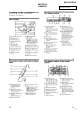
MZ-G750/R700 SECTION 2 GENERAL This section is extracted from instruction manual.
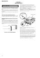
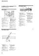
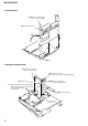
MZ-G750/R700 (MZ-R700) 6
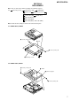
MZ-G750/R700 SECTION 3 DISASSEMBLY Note : This set can be disassemble according to the following sequence. Set Panel Assy,Lower Panel Assy, Upper Main Board LCD Module MD Mechanism Deck Service Assy, OP Holder Assy Motor Flexible Board Motor, DC (M602) Motor, DC (M601), Motor, DC (M603) Note : Follow the disassembly procedure in the numerical order given. 3-1. PANEL ASSY, LOWER 3 screws (1.4x2.0), MI 4 claw 2 screws (1.4x2.0), MI 1 6 Panel Assy , Lower 5 3-2. PANEL ASSY, UPPER 2 screws (1.
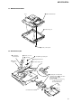
MZ-G750/R700 3-3. LCD MODULE 2 screws (1.7x2.5) 1 screws (1.7x2.5) 4 LCD module 3 claws panel assy, upper 3-4. MAIN BOARD 8 CN501 4 screws (M1.7x3) 6 Remove the solders 2 arm 3 screws (M1.4x2) qa Remove the solder 7 qd MAIN board 5 screws (M1.
MZ-G750/R700 3-5. MD MECHANISM DECK 3 MD mechanism deck boss boss 2 chassis assy, set 1 screws (1.4x1.6), MI 3-6. SERVICE ASSY, OP 3 screw(M1.4), precision pan 1 washer (0.8 - 2.5) 5 screw(M1.4), precision pan 2 gear (SA) 6 spring, thrust detent 4 spring(s), pack 8 Pull off the lead screw. 7 9 Opening the over write head toward the direction A, remove the OP Service assy toward the direction B. Note: Do not open the entire assy forcibly, when opening the over write head.
MZ-G750/R700 3-7. HOLDER ASSY 4 Remove the holder assy to direction of the arrow B. 1 Open the holder assy. A 2 B 3 boss 3-8. MOTOR FLEXIBLE BOARD 1 Remove four solders of DC motor (sled) (M602). 2 Remove two solders of DC motor (over write head up/down) (M603). 4 adhesive sheet 3 Remove four solders of DC motor (spindle) (M601). Note: Align a circular hole in the stripping paper with a circular hole in the DC motor (sled), when mounting the motor flexible board.
MZ-G750/R700 3-9. MOTOR, DC (M602) 3 Remove four solders of motor flexible board. 4 two screws(M1.4), precision pan 1 washer (0.8 - 2.5) 2 gear (SA) 5 moter, DC (sled) (M602) 3-10. “MOTOR, DC (M601)”, “MOTOR, DC (M603)” 1 Remove six solders of motor flexible board. Note: Press-fit the gear (HA) up to the position of the DC motor (over write head up/down) (M603) as shown below. qs moter, DC (over write head up/down) (M603) gear (HA) 6 two screws(M1.4), precision pan 4 three screws(M1.
MZ-G750/R700 SECTION 4 TEST MODE 4-1. Outline 4-3. Operation in Setting the Test Mode • This set provides the Overall adjustment mode that allows CD and MO discs to be automatically adjusted when in the test mode. In this overall adjustment mode, the disc is discriminate between CD and MO, and each adjustment is automatically executed in order. If a fault is found, the system displays its location. Also, the manual mode allows each individual adjustment to be automatically adjusted.
MZ-G750/R700 4-5. Configuration of Test Mode Major item switching Test mode (Display Check Mode) Press the > or VOL+ key N key Manual Mode Press the x key x key Servo Adjustment Press the . or VOL– Audio Adjustment Power Supply Adjustment Medium item switching OP Alignment Adjustment N key VOL – key: 100th Place of item number decrease. VOL + key: 10th Place of item number increase. VOL – key: 10th Place of item number decrease.
MZ-G750/R700 5. The display changes a shown below each time the [ENTER] key on the set is pressed. • Address & Adjusted Value Display This set LCD display 3A4S1D adjustment value address 0 11 item number • Jitter Value & Adjusted Value Display This set LCD display 0FEJ1D adjustment value jitter value 0 11 item number • Block Error Value & Adjusted Value Display This set LCD display 063B1D 0 11 4-8.
MZ-G750/R700 • Description of Error Indication Codes Problem No error Servo system error TOC error Power supply system error Offset system error Indication code Meaning of code Simple display Description 00 No error --- No error 01 Illegal access target address was specified Adrs Attempt to access an abnormal address 02 High temperature Temp High temperature 03 Focus error Fcus Disordered focus 04 Spindle error Spdl Abnormal rotation of disc 11 TOC error TOC Faulty TOC conten
MZ-G750/R700 4-10. Sound Skip Check Result Display Mode • Cause of Sound Skip Error This set can display the count of errors that occurred during the recording/playing for checking. Cause of error EIB • Setting method of sound skip check result display mode 1. Set the test mode (see page 12). 2. Press the N key or [REC] key, and the playing or recording sound skip result display mode becomes active respectively where the LCD displays the following.
MZ-G750/R700 4. When all the keys on the set and on the remote commander are considered as OK, the following displays are shown for 4 seconds. Example1: When the keys on the set are considered as OK: This set LCD display SET OK 0 00 : AD value of the remote commander Key (hexadecimal OO to FF) Example2: When the keys on the remote commander are considered as OK: This set LCD display RMC OK 0 00 : AD value of the remote commander Key (hexadecimal OO to FF) 5.
MZ-G750/R700 SECTION 5 ELECTRICAL ADJUSTMENTS 5-1. Outline • In this set, automatic adjustment of CD and MO can be performed by entering the test mode (see page 12). However, before starting automatic adjustment, the memory clear, power supply adjustment, and laser power check must be performed in the manual mode. • A key having no particular description in the text, indicates a set key. • For the LCD display, the LCD display on the set is shown. • Setting method of NV reset 1.
MZ-G750/R700 3) Press the X key to write the adjusted value. 4) Select the manual mode of the test mode, and set item number 862 (see page 13). This set LCD display V1dat 8 62 • Adjustment method of Vc PWM Duty (L) (item number: 762) This set LCD display VclPWM 7 62 : Adjusted value : Adjusted value 5) Adjust with the [VOL+] key (adjusted value up) or [VOL--] key (adjusted value down) so that the adjusted value becomes 01. 6) Press the X key to write the adjusted value.
MZ-G750/R700 1. Connect a digital voltmeter to the TP902 (VL) on the MAIN board, and adjust [VOL +] key (voltage up) or [VOL --] key (voltage down) so that the voltage becomes 2.30 ± 0.01 V. digital voltmeter 2. Press the . key continuously until the optical pick-up moves to the most inward track. 3. Open the cover and set the laser power meter on the objective lens of the optical pick-up. 4. Press the N key, and set the laser MO read adjustment mode (item number 011).
MZ-G750/R700 Adjustment/checking and Connection Location: 5-8. Overall Adjustment Mode • Configuration of overall adjustment –MAIN BOARD(SIDE A)– Overall adjustment mode (Title display) N key Protect switch ON .
MZ-G750/R700 • Overall Adjustment Mode (Title Display) This set LCD display Assy 0 00 • Adjustment Method of Overall CD and MO Adjustment Mode 1. Setting the test mode (see page 12). 2. Press the . or [VOL --] key activates the overall adjustment mode. This set LCD display : (Disc mark) At end power supply adjustment:Outside lit At end of electrical offset adj.:inside lit Note:On the set having microcomputer version 1.000,the disc mark is displayed on the set LCD only.
MZ-G750/R700 • Overall CD and MO adjustment items 1. Overall CD adjustment items Item No. 312 313 CD electrical offset adjustment CD tracking error gain adjustment 328 CD TWPP gain adjustment 0 43 2. Press the X key. CD ABCD gain adjustment 344 CD focus gain adjustment 345 CD tracking gain adjustment 522 Resume CC CD tracking error offset adjustment 336 521 • Resume Clear Setting Method 1. Select the manual mode of the test mode, and set item number 043 (see page 13).
MZ-G750/R700 • Modified Data Writing Method (version 1.000) 1. Select the manual mode of the test mode, and set item number 023 (see page 13). This set LCD display This set LCD display Patch 00 0 23 0 23 13. Press the X key. (0D5E is blinking) 14. Press the [VOL+] key once to change the blinking portion to 0D5F. This set LCD display This set LCD display 0 23 0D5F00 0 23 00: Adjusted value 00: Adjusted value 4.
MZ-G750/R700 This set LCD display 0D61A1 This set LCD display 0 23 A1: Adjusted value 0 23 DD: Adjusted value 25. Press the X key. (0D61 is blinking) 26. Press the [VOL+] key once to change the blinking portion to 0D62. This set LCD display 0D6200 SDD 0 23 37. Turn the power off. • Modified Data Writing Method (version 1.100) 1. Select the manual mode of the test mode, and set item number 023 (see page 13). This set LCD display Patch 00 0 23 00: Adjusted value 27. Press the x key.
MZ-G750/R700 This set LCD display 0D5E04 0 23 This set LCD display 04: Adjusted value 12. Press the X key. (0D5E is blinking) 13. Press the [VOL+] key to change the blinking portion to 0D61. This set LCD display 0D6100 0 23 00: Adjusted value 14. Press the x key. (00 is blinking) 15. Adjust with the [VOL+] key (adjusted value up) or [VOL--] key (adjusted value down) so that the adjusted value becomes 20. This set LCD display 0D6120 0 23 16. Press the X key. (0D61 is blinking) 17.
MZ-G750/R700 36. Press the X key. (0D69 is blinking) 37. Press the [VOL+] key to change the blinking portion to 0D6C. This set LCD display 0D6C00 This set LCD display 0 23 00: Adjusted value This set LCD display 0 23 0 23 42. Press the x key. (00 is blinking) 43. Adjust with the [VOL+] key (adjusted value up) or [VOL--] key (adjusted value down) so that the adjusted value becomes 1C. This set LCD display 52. Press the X key. (0D72 is blinking) 53.
MZ-G750/R700 60. Press the X key. (0D65 is blinking) 61. Press the [VOL+] key once to change the blinking portion to 0D75. This set LCD display This set LCD display 0D7500 0 23 62. Press the x key. (00 is blinking) 63. Adjust with the [VOL+] key (adjusted value up) or [VOL--] key (adjusted value down) so that the adjusted value becomes 1C. 0 23 74. Press the x key. (00 is blinking) 75.
MZ-G750/R700 SECTION 6 DIAGRAMS 6-1. IC PIN FUNCTION DESCRIPTION • IC501 SN761057DBT (RF AMP, FOCUS/TRACKING ERROR AMP) Pin No.
MZ-G750/R700 • IC801 CXD2671-204GA (SYSTEM CONTROLLER, DIGITAL SIGNAL PROCESSOR, 16M BIT D-RAM) Pin No. Pin Name I/O Description 1 PAUSE KEY I Set key input terminal (X key input) 2 MIC SENSE O Control signal output to the microphone amp “H”: HIGH, “L”: LOW, normally: “H” (Not used) 3 4, 5 XTEST NC I O Input terminal for the test mode set up Not used (open) 6 7 MCUVDD0 MIFVSS3 — — Power supply terminal (for microcomputer block) (+1.
MZ-G750/R700 Pin No. 52 Pin Name AVD2 I/O — Description Power supply terminal (for the analog) (+2.4 V) 53 54 AVS2 ADRB — I Ground terminal (for the analog) A/D converter the lower limit voltage input (fixed at “L” in this set) 55 56 SE TE I I 57 58 DCHG APC — I Connecting analog power supply of the low impedance (fixed at “H” in this set) Error signal input for the laser automatic power control Not used (fixed at “H”) 59 60 DSPVDD0 DSPVSS0 — — Power supply terminal (for DSP block) (+1.
MZ-G750/R700 Pin No. Pin Name I/O 99 SLDW O 100 SLCU I output (2+) Spindle motor drive comparison signal input (U) from the motor driver (IC551) 101 102 SLCV SLCW I I Spindle motor drive comparison signal input (V) from the motor driver (IC551) Spindle motor drive comparison signal input (W) from the motor driver (IC551) 103 104 DIFVDD1 DIFVSS1 — — Power supply terminal (for DSP I/F) (+2.
MZ-G750/R700 Pin No.
MZ-G750/R700 Pin No. 224 – 226 Pin Name (XAVLS), (SOUND 1, 2) I/O I 227 228 XHOLD SW (SYCN REC) I I HOLD switch input terminal “L”: hold ON, “H”: hold OFF SYNCHRO REC switch input terminal “L”: OFF, “H”: ON 229 NC O 230 PROTECT I Not used (open) Detection input terminal of the record check claw from the protect detection switch 231 FLASHVDD — (S803) “L”: recording possible condition, “H”: protect Power supply terminal (for the internal FLASH ROM) (+2.
MZ-G750/R700 6-2.
MZ-G750/R700 6-3.
MZ-G750/R700 6-4.
MZ-G750/R700 6-5. PRINTED WIRING BOARD — MAIN SECTION — 2 3 4 5 6 7 8 9 Note: • Y : parts extracted from the conductor side. • : Pattern from the side which enables seeing. (The other layer’s patterns are not indicated.) A S805 (HALF LOCK) B Parts on the pattern face side seen from the pattern face are indicated. Parts on the parts face side seen from the parts face are indicated.
MZ-G750/R700 13 12 11 10 9 8 7 6 5 4 3 S803 (PROTECT DETECT) • Semiconductor Location (SIDE B) C MD MECHANISM S G750 5 10 D G L1002 C1006 AP806 AP807 AP810 AP808 AP814 AP809 C809 C814 AP848 FB801 R806 C808 C807 R1028 R700 1 42 40 43 R606 TP611 8 35 D1005 C618 50 3 25 IC601 20 AP601 R620 10 R801 4 8 ! 39 39 C813 C817 C608 5 4 Q605 15 14 C622 C609 D606 AP602 C623 56 1 5 IC1006 G750 R613 C607 AP606 1 C619 29 28 45 R624 6 7 R825 L1003 C610
MZ-G750/R700 Common note on Schematic Diagram: • All capacitors are in µF unless otherwise noted. pF: µµF 50 WV or less are not indicated except for electrolytics and tantalums. • All resistors are in Ω and 1/4 W or less unless otherwise specified. • % : indicates tolerance. • C : panel designation. Note: The components identified by mark 0 or dotted line with mark 0 are critical for safety. Replace only with part number specified.
MZ-G750/R700 6-6. SCHEMATIC DIAGRAM — MAIN SECTION (1/3) — • Refer to page 40 for Waveforms. Refer to page 44 for IC Block Diagrams.
MZ-G750/R700 6-7. SCHEMATIC DIAGRAM — MAIN SECTION (2/3) — • Refer to page 40 for Waveforms. Refer to page 44 for IC Block Diagrams.
MZ-G750/R700 6-8. SCHEMATIC DIAGRAM — MAIN SECTION (3/3) — • Refer to page 44 for IC Block Diagrams. * R104,204 14 13 12 11 10 9 Except US model:10k US model: 33k 8 3 2 1 * 1 2 3 4 5 6 7 IC B/D 4 * C101,201 Except US model:2.2 US model: 0.
MZ-G750/R700 • IC BLOCK DIAGRAMS VREF 4 C 5 D 6 TE S-MONITOR TEMP RO3 PGND3 FO3 VM34 RO4 PGND4 FO4 40 39 38 37 36 35 34 33 32 31 30 29 – + 28 VM4 VC – + VC VG VG PRE DRIVER PRE DRIVER VG VC PGNDW 43 VC VC H-BRIDGE CONTROL WO 44 VMVW 45 H-BRIDGE CONTROL PRE DRIVER TE 1 REXT 2 Wpp LPF 3 TWpp PK/BTM Aw CSLO VREF075 A-C D-C Malfa Mij AwBPF Dw DwBPF VM3 43 S-MON A+B+C+D I+J NPP TON CSL Aw+Dw TON Peak TON Botm ADIP TE CPBO 42 41 44 ADIP-IN CPAO SC111257FCR2 CPBIP CPBIM
MZ-G750/R700 VRECIN2 VG HB PGND3 HA 39 38 37 36 35 34 33 VG3 VG OUTPUT SW VGC VC2 VC EFM PRE DRIVER CONTROL 28 C1H 27 C1L CHARGE PUMP 1 CHARGE PUMP 2 26 VC2 VREF BUFFER VG3 DC IN 29 VC2 VG VG3 VC HI-BRIDGE PRE DRIVER CHARGE MONITOR X2/X4 BATM 44 32 31 30 OUTPUT SW VC VG DC IN VB 43 VG2 VG2 OUTB 40 C2L PGND2 41 C2H PGND2 42 VG3 OUTA XPC18A22FCR2 VRECIN1 IC601 25 VREF 24 CVREF CONTROL 23 GND CHARGE CONTROL CHGSW 45 22 DW BT 21 DW TP DC IN 46 47 48 49 VC
MZ-G750/R700 IC301 AK5354VT 16 PDN CONTROL REGISTER I/F 15 CSN 14 CCLK 13 CDTI 12 LRCK 11 MCLK CLOCK DIVIDER LIN1 1 10 BCLK IPGA ADC HPF AUDIO I/F CONTROLLER RIN1 2 LIN2 3 RIN2 4 VCON VCON 5 AGND 6 VA 7 VA VD 8 VD GND VREF IN 18 17 16 15 14 13 PW SW MT SW BST SW BEEP STB MUTE BEEP TA2131FL BST SW IC302 V REF 12 VREF 11 LPF1 TCMT 19 VCC 20 ADD IN R 21 10 NF1 BST1 IN L 22 9 LPF2 PW A OUTB BEEP 23 PW B BST2 8 NF2 7 BST OUTA BEEP 24 46 1 2 3 4 5 6 +B OUT L
MZ-G750/R700 SECTION 7 EXPLODED VIEWS NOTE: • The mechanical parts with no reference number in the exploded views are not supplied. • Items marked “*” are not stocked since they are seldom required for routine service. Some delay should be anticipated when ordering these items. • -XX and -X mean standardized parts, so they may have some difference from the original one. • Color Indication of Appearance Parts Example : KNOB, BALANCE (WHITE) ...
MZ-G750/R700 7-2. CHASSIS SECTION MT-MZR700-172 51 60 55 52 54 56 @ 53 59 58 56 57 Ref. No. Part No. 51 52 * 53 * 53 X-3379-555-1 CHASSIS ASSY, SET 3-222-779-01 SPRING (OPEN), TENSION A-3323-650-A MAIN BOARD, COMPLETE (R700:CND,AEP,UK,E, AUS,EE,JE,FR,AR,HK,CH,TW,KR) A-3323-652-A MAIN BOARD, COMPLETE (G750:AEP,UK,E,AUS, CET,JE,FR,HK,KR) A-3323-694-A MAIN BOARD, COMPLETE (R700:US) * 53 A-3323-703-A MAIN BOARD, COMPLETE (G750:US) * 53 48 Description Remark Ref. No. Part No.
MZ-G750/R700 7-3. MD MECHANISM DECK SECTION (MT-MZR700-172) 101 117 119 120 118 102 105 103 106 B B A A 104 108 M603 107 115 109 121 122 110 112 M602 111 M601 115 103 109 103 113 109 Ref. No. 114 116 The components identified by mark 0 or dotted line with mark 0 are critical for safety. Replace only with part number specified. 109 Part No. Description 101 102 103 104 105 X-3379-515-1 3-224-779-01 4-963-883-42 X-3379-514-1 4-222-218-02 HOLDER ASSY SPRING, THRUST DETENT SCREW (M1.
MZ-G750/R700 SECTION 8 ELECTRICAL PARTS LIST MAIN NOTE: • Due to standardization, replacements in the parts list may be different from the parts specified in the diagrams or the components used on the set. • -XX and -X mean standardized parts, so they may have some difference from the original one. • RESISTORS All resistors are in ohms. METAL:Metal-film resistor. METAL OXIDE: Metal oxide-film resistor.
MZ-G750/R700 MAIN Ref. No. Part No. Description Part No. Description C521 C522 C523 C524 C527 1-125-777-11 1-125-777-11 1-125-837-11 1-135-259-11 1-119-923-11 CERAMIC CHIP CERAMIC CHIP CERAMIC CHIP TANTAL. CHIP CERAMIC CHIP 0.1uF 0.1uF 1uF 10uF 0.047uF 10% 10% 10% 20% 10% 10V 10V 6.3V 6.3V 10V Remark Ref. No. C808 C809 C810 C811 C812 1-164-850-11 1-135-259-11 1-125-837-11 1-125-837-11 1-164-943-11 CERAMIC CHIP TANTAL. CHIP CERAMIC CHIP CERAMIC CHIP CERAMIC CHIP 10PF 10uF 1uF 1uF 0.01uF 0.
MZ-G750/R700 MAIN Ref. No. Part No. Description Remark C1007 1-117-919-11 TANTAL. CHIP 10uF 20% C1008 1-117-919-11 TANTAL. CHIP 10uF 20% C1009 1-117-919-11 TANTAL. CHIP 10uF 20% C1010 1-127-895-11 TANTAL. CHIP 22uF 20% C1011 1-127-895-11 TANTAL. CHIP 22uF 20% C1012 1-164-943-11 CERAMIC CHIP 0.01uF 10% C1016 1-137-762-11 TANTALUM 10uF 20% Ref. No. Part No. Description 1-216-864-11 SHORT 1-216-864-11 SHORT Remark 6.3V (G750) 6.3V (G750) 6.
MZ-G750/R700 MAIN Ref. No. Part No. Description Part No. Description Q302 Q501 Q601 Q602 Q603 8-729-046-49 8-729-922-10 8-729-046-45 8-729-046-44 8-729-053-71 FET FDV304P TRANSISTOR 2SA1577-QR FET SI2302DS-T1 TRANSISTOR ZDT6718TA FET TS8K1TB Remark R317 R318 R319 R501 R505 1-218-941-11 1-218-953-11 1-218-953-11 1-218-971-11 1-208-703-11 RES-CHIP RES-CHIP RES-CHIP RES-CHIP METAL CHIP 100 1K 1K 33K 6.8K 5% 5% 5% 5% 0.
MZ-G750/R700 MAIN Ref. No. Part No. Description R837 R839 R840 R841 R902 1-218-990-11 1-208-939-11 1-216-809-11 1-218-990-11 1-218-985-11 SHORT METAL CHIP METAL CHIP SHORT RES-CHIP 0 150K 100 0 470K Remark R903 R905 R906 R907 R908 1-218-957-11 1-218-957-11 1-218-990-11 1-218-985-11 1-218-977-11 RES-CHIP RES-CHIP SHORT RES-CHIP RES-CHIP R909 R910 R911 R914 R915 1-218-965-11 1-218-965-11 1-218-949-11 1-218-941-11 1-216-296-11 RES-CHIP RES-CHIP RES-CHIP RES-CHIP SHORT 0.
MZ-G750/R700 Ref. No. Part No.
MZ-G750/R700 REVISION HISTORY Clicking the version allows you to jump to the revised page. Also, clicking the version at the upper right on the revised page allows you to jump to the next revised page. Ver. 1.1 1.0 56 Date 2001. 02 2001. 01 Description of Revision US, Canadian, E, Australian and Chinese model has been added.