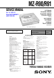
MZ-R90/R91 SERVICE MANUAL US Model Canadian Model Australian Model Chinese Model Ver 1.4 2001.01 With SUPPLEMENT-1 (9-927-187-83) MZ-R90 AEP Model UK Model E Model Tourist Model MZ-R90/R91 Photo: MZ-R91 (Blue type) US and foreign patents licensed from Dolby Laboratories Licensing Corporation.
TABLE OF CONTENTS 1. SERVICING NOTES ............................................... 3 2. GENERAL ................................................................... 4 3. DISASSEMBLY ......................................................... 5 4. TEST MODE .............................................................. 11 5. ELECTRICAL ADJUSTMENTS ......................... 18 6. DIAGRAMS 6-1. Block Diagram –SERVO Section– ................................. 6-2.
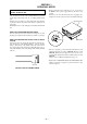
SECTION 1 SERVICING NOTES NOTES ON HANDLING THE OPTICAL PICK-UP BLOCK OR BASE UNIT The laser diode in the optical pick-up block may suffer electrostatic break-down because of the potential difference generated by the charged electrostatic load, etc. on clothing and the human body. During repair, pay attention to electrostatic break-down and also use the procedure in the printed matter which is included in the repair parts. The flexible board is easily damaged and should be handled with care.
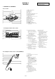
SECTION 2 GENERAL This section is extracted from instruction manual. • LOCATION OF CONTROLS – The recorder – 0 1 qa 2 qs 3 qd 4 qf 5 1 2 3 4 5 6 7 8 9 ql 0 qa qs qd qf qg qh qj qk ql 1 8 1 2 9 3 0 qg 6 qh 7 qj 8 qk 9 x (stop) /CHARGE button Display window REC indicator DC IN 3V jack Jog lever i/LINE OUT (headphones/line out) jack MIC (PLUG IN POWER) jack LINE IN (OPTICAL) jack HOLD switch Slide to lock the controls of the recorder.
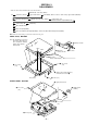
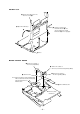
SECTION 3 DISASSEMBLY • This set can be disassembled in the order shown below.
LCD MODULE, “BUTTON, CONTROL”, “SERVICE ASSY, UPPER PANEL” • MZ-R90 1 five screws (1.4) 2 LCD module 3 control button 4 upper panel service assy • MZ-R91 1 five tapping screws (1.7) 2 LCD module 3 control button Note: The control buttons are stuck with strong adhesive sheets. As the control buttons are very fragile, do not peel them off forcibly.
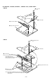
MAIN BOARD, “CASE ASSY, BATTERY” 2 flexible board (LCD module) (CN801) 2 flexible board (over write head) (CN601) 1 Remove the solder of joint. 3 four toothed lock screws (M1.4) 1 Remove the solder of battery terminal (minus). 4 6 main board 8 batter case assy 1 Remove the solder of battery terminal (plus). 2 motor flexible board (CN602) 5 flexible board (optical pick-up) (CN501) Note: Before removing the flexible board from CN501, be sure to solder the flexible board.
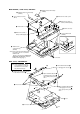
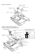
“CHASSIS ASSY, SET”, MD MECHANISM DECK (MT-MZR90-165) 3 MD mechanism deck (MT-MZR90-165) 2 boss 2 boss 4 tension spring (arm) 1 screw (1.4) 5 set chassis assy 1 screw (1.4) SERVICE ASSY, OP 1 washer (0.8 - 2.5) 3 precision pan screw (M1.4) 2 gear (SA) 7 Pull off the lead screw. 4 rack spring 5 screw 5 screw 6 8 bearing 9 Opening the over write head toward the direction A, remove the OP Service assy toward the direction B.
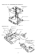
HOLDER ASSY 5 Remove the holder assy in the direction of arrow C. B 1 Open the holder assy. 2 Push the convex portion toward the direction B and open the holder assy toward the direction A to erect uprightly. A 3 C 4 boss MOTOR FLEXIBLE BOARD 1 Remove four solders of DC motor (sled) (M602). 1 Remove two solders of DC motor (over write head up/down) (M603). 1 Remove four solders of DC motor (spindle) (M601).
MOTOR, DC (SLED) (M602) 1 Remove four solders of motor flexible board. 2 washer (0.8 - 2.5) 4 two precision pan screws (M1.4) 3 gear (SA) 5 DC motor (sled) (M602) “MOTOR, DC SSM-01C14A (SPINDLE) (M601)”, “MOTOR, DC (OVER WRITE HEAD UP/DOWN) (M603)” 1 Remove six solders of motor flexible board. qa DC motor (over write head up/down) (M603) Note: Press-fit the gear (HA) up to the position of the DC motor (over write head up/down) (M603) as shown below. gear (HA) 6 two precision pan screws (M1.
SECTION 4 TEST MODE [Outline] • This set provides the Overall adjustment mode (Assy mode) that allows CD and MO disc to be automatically adjusted when in the test mode. In this overall adjustment mode, the protect switch is detected to judge the disc, CD or MO, and each adjustment is automatically executed in order. If a fault is found, the system displays its location. Also, the manual mode allows each individual adjustment to be automatically adjusted.
[VOL +] key:100th place of mode number [Configuration of Test Mode] [Major item switching] [Test Mode $Display Check Mode%] Press the > or [VOL +] key [Manual Mode] Press the x key increase. [VOL --] key:100th place of mode number N key [Servo Mode] [Audio Mode] [Power Mode] [OP Alignment Mode] x key decrease. [VOL +] key:10th place of mode number increase. [Medium item switching] [VOL --] key:10th place of mode number N key x key decrease. Press the .
5. The display changes a shown below each time the jog key on the set is turned up or [DISPLAY] key on the remote commander is pressed. [Overall Adjustment Mode] Mode to adjust the servo automatically in all items. Normally, automatic adjustment is executed in this mode at the repair. Adjust the CD first, when performing adjustment. • Configuration of overall adjustment • Address & Adjusted Value Display > key LCD display 011 C68S01 Title display .
[Sound Skip Check Result Display Mode] This set can display and check the error count occurring during record and play. • Setting method of Sound Skip Check Result Display Mode 1. Setting the test mode. (See page 11) 2. Press the N or [REC] key on the set activates the sound skip check result display mode where the LCD displays as shown below. If microprocessor version is 1.20 When N key is pressed: 4.
[Self-Diagnosis Display Mode] • This set uses the self-diagnosis system in which if an error occurs in recording/playback mode, the error is detected by the model control and power control blocks of the microprocessor and information on the cause is stored as history in EEPROM. By viewing this history in test mode, it helps you to analyze a fault and determine its location.
• Description of Indication History History code number Description 1st0 The first error 1st1 Total recording time when 1st0 was generated (Higher rank byte) 1st2 Total recording time when 1st0 was generated (Lower rank byte) N0 The last error N1 Total recording time when N 0 was generated (Higher rank byte) N2 Total recording time when N 0 was generated (Lower rank byte) N-10 One error before the last.
[Key Check Mode] This set can check if the set and remote commander function normally. • Setting Method of Key Check Mode 1. Setting the test mode. (See page 11) 2. Press the [T MARK] or [DISPLAY] key on the remote commander for several seconds activates the key check mode where all segments of LCD turn OFF. (At the last two digits of DOT section, AD value of remote commander key line is displayed in hexadecimal) 3.
Ver 1.4 2001. 01 SECTION 5 ELECTRICAL ADJUSTMENTS [Outline] [NV Reset] • In this set, automatic adjustment of CD and MO can be performed by entering the test mode. (See page 11) However, before starting automatic adjustment, the memory clear, power adjustment and temperature adjustment must be performed in the manual mode. • The keys in the description refer to the keys on both set and remote commander unless otherwise specified.
• Adjustment method of VC PWM Duty (L) (mode number: 762) 1. Select the manual mode of the test mode, and set the mode number 762. (See page 12) • Adjustment method of VC PWM Duty (H) (mode number: 765) 1. Select the manual mode of the test mode, and set the mode number 765. (See page 12) LCD display 762 LCD display VclPWM 765 2. Connect a digital voltmeter to the TP915 (VC) on the MAIN board, and adjust [VOL +] key (voltage up) or [VOL --] key (voltage down) so that the voltage becomes 2.5 ± 0.02 V.
• CD Automatic Adjustment item [Temperature Correction] • Adjustment Method of temperature correction 1. Select the manual mode of test mode, and set the mode number 014. (See page 12) Mode No. Description 312 313 LCD display CD electrical offset adjustment 314 SetTmp 014 328 CD TWPP gain adjustment 321 CD tracking error gain adjustment 323 2. Measure the ambient temperature. 3. Adjust with [VOL +], [VOL --] key so that the adjusted value (hexadecimal value) becomes the ambient temperature.
Ver 1.4 2001. 01 • MO Automatic Adjustment item Mode No. 14. When both CD and MO overall adjustments are OK, set the manual mode and clear the clock data. For the microprocessor version 1.20 or later, set the mode number 043 (Resume), and press the X key.
MZ-R90/R91 SECTION 6 DIAGRAMS HA CK RF AMP, FOCUS/TRACKING ERROR AMP IC501 PEAK/ BOTM B C D IX BOTM 33 18 29 SAW. GEN.
MZ-R90/R91 6-2. 6-3.
MZ-R90/R91 Ver 1.2 2000. 02 6-4. PRINTED WIRING BOARD • Semiconductor Location Ref. No.
6-5. SCHEMATIC DIAGRAM • See page 38 for Waveforms. – 33 – MZ-R90/R91 • See page 41 for IC Block Diagrams.
• Waveforms qg IC601 ej, ek, el, r; (COM, CPWI, CPVI, CPUI) 400 mV/DIV, 5 µs/DIV wg Q607 (Drain) 50 mV/DIV, 5 µs/DIV w; IC801 yh (VC PWM) 40 mV/DIV, 5 µs/DIV • IC Block Diagrams 2.8 Vp-p LIN1 RIN1 TST1 LIN2 RIN2 114 mVp-p 203 mVp-p 1.3 Vp-p PD RST SSB NC NC NC Approx. 1.4 Vp-p 2.
VC VI 1 UI 2 PWM 3 GNDUV VO VMVW WO GNDW CPUI CPVI CPWI COM 47 46 45 44 43 42 41 40 39 38 37 VG VC 3PHASE CONTROL UO 48 VMU MPC17A56FTA WI IC601 PRE DRIVER + – 36 CPUO + – 35 CPVO + – 34 CPWO VM1 4 VG VC VC VC VG VC 33 VM3 RO1 5 PGND1 6 FO1 7 VM12 8 PRE DRIVER VG VC H-BRIDGE CONTROL H-BRIDGE CONTROL VC VC VC RO2 9 PGND2 10 FO2 11 PRE DRIVER VG VC ROE 29 VM34 BIAS PRE DRIVER 32 RO3 31 PGND3 30 FO3 H-BRIDGE CONTROL H-BRIDGE CONTROL PRE DRIVER 28
SS DTC NC PGNDLG VB VIN C1H VGH C1L VCC CK COSC MODE 1 MODE 2 MPC18A20MTAEL RF IC603 30 29 28 27 26 25 24 23 22 21 20 19 18 17 16 CLK SAW CONTROL LOGIC CHARGE PUMP PRE DRIVER OSC EN ENB SAW GEN COMP + CLK SAW VREF PRE DRIVER COMP EFM LOGIC BIAS OP IC605 6 7 8 9 10 11 ERRIV GND VSET VG VGI PGNDG PGNDB HB HA XC6367B103MR 12 IC803 CE 1 SLOW START 13 14 15 VERF 5 EFM 4 GND 3 PGNDA 2 ERRID INM 1 VREF XC6383C301MR CHIP ENABLE VDD VLX LI
IC804 32K OUT RV5C348A-E2 32KHz OUTPUT CONTROL 1 10 VDD ALARM W REGISTER (WEEK,MIN,HOUR) COMPARATOR W ALARM D REGISTER (MIN,HOUR) COMPARATOR D VOLTAGE DETECT 9 OSC IN TIME COUNTER (SEC,MIN,HOUR,WEEK,DAY,MONTH,YEAR) SCLK 3 SI 4 8 OSC OUT ADDRESS DECORDER ADDRESS REGISTER I/O CONTROL 7 CE OSC DETECT SHIFT REGISTER 6 /INTR INTERRUPT CONTROL 5 CHGMON VREF VB CLK RSTREF CRST XRST VRMC VBTB FFCLR 48 VB DCIN CHGB MPC18A31FTA CHGSW IC901 OSC 2 SO VSS DIVIDER CORRECTION DI
6-6. IC PIN FUNCTION DESCRIPTION • MAIN BOARD IC501 SN761056ADBT (RF AMP, FOCUS/TRACKING ERROR AMP) Pin No. Pin Name I/O 1 TE O Description Tracking error signal output to the CXD2660GA (IC502) 2 REXT — Connected to the external resistor for the ADIP amplifier control 3 WPPLPF — Connected to the external capacitor for low-pass filter of the TPP/WPP 4 VREF11 O Reference voltage output terminal (+1.
• MAIN BOARD IC502 CXD2660GA (DIGITAL SIGNAL PROCESSOR, DIGITAL SERVO SIGNAL PROCESSOR, EFM/ACIRC ENCODER/DECODER, SHOCK PROOF MEMORY CONTROLLER, ATRAC ENCODER/DECODER, 16M BIT D-RAM) Pin No. Pin Name I/O 1 VDC0 — Power supply terminal (+1.
Pin No. Pin Name I/O Description 46 FS256 O Clock signal (11.2896 MHz) output to the A/D, D/A converter (IC301) (X' tal system) 47 to 52 A03, A04, A02, A05, A01, A06 O Address signal output to the external D-RAM 53 VDIO1 — Power supply terminal (+2.4V) (for I/O) 54 VSIO1 — Ground terminal (for I/O) 55 to 59 A00, A07, A10.
Pin No. Pin Name I/O Description 103 XLRF O Serial latch signal output terminal Not used (open) 104 CKRF O Serial clock signal output terminal Not used (open) 105 DTRF O Writing data output terminal Not used (open) 106 APCREF O Control signal output to the reference voltage generator circuit for the laser automatic power control 107 LDDR O PWM signal output for the laser automatic power control Not used (open) 108 VDC4 — Power supply terminal (+1.
• MAIN BOARD IC801 CXR701080-013GA (MASTER CONTROLLER) Pin No.
Pin No. Pin Name I/O Description 39 FFCLR O Input latch output for starting signal to the MPC18A31FTA (IC901) 40 SLEEP O System sleep control signal output to the MPC18A31FTA (IC901) “H”: sleep on 41 TSB EDGE I TSB slave edge detect signal input terminal 42 GND SW O Ground line switching signal output terminal 43 XRST I System reset signal input from the MPC18A31FTA (IC901) “L”: reset For several hundreds msec.
Pin No.
SECTION 7 EXPLODED VIEWS NOTE: • Items marked “*” are not stocked since they • -XX and -X mean standardized parts, so they are seldom required for routine service. Some may have some difference from the original delay should be anticipated when ordering one. these items. • Color Indication of Appearance Parts • The mechanical parts with no reference numExample: ber in the exploded views are not supplied. KNOB, BALANCE (WHITE) . . .
(2) PANEL SECTION (MZ-R91) 54 53 chassis section 60 53 not supplied not supplied 53 57 53 59 53 60 58 59 52 51 Ref. No. Part No. Description 51 51 51 52 52 4-223-077-21 4-223-077-31 4-223-077-41 X-4952-184-1 X-4952-186-1 LID, BATTERY CASE (BLUE) LID, BATTERY CASE (RED) LID, BATTERY CASE (WHITE) PANEL (L) ASSY, BOTTOM (BLUE) PANEL (R) ASSY, BOTTOM (RED) 52 53 X-4952-188-1 PANEL (W) ASSY, BOTTOM (WHITE) 4-218-229-09 SCREW (1.4), MI Remark Ref. No. Part No.
(3) CHASSIS SECTION 101 MT-MZR90-165 102 103 105 104 113 112 105 114 106 108 110 107 111 109 R91 not supplied Ref. No. 101 101 102 103 104 105 106 107 107 107 Part No. Description 110 Remark 109 Ref. No. Part No. Description Remark MAIN BOARD, COMPLETE (R90: US, CND) TERMINAL (3) SCREW (M1.
(4) MD-MECHANISM DECK SECTION (MT-MZR90-165) 165 166 167 168 164 R91 169 177 167 154 163 152 171 162 153 170 173 172 161 154 160 154 159 174 158 M602 157 152 153 M601 156 M603 175 154 155 152 The components identified by mark 0 or dotted line with mark 0 are critical for safety. Replace only with part number specified. 151 Les composants identifiés par une marque 0 sont critiques pour la sécurité. Ne les remplacer que par une pièce portant le numéro spécifié. 176 Ref. No. Part No.
SECTION 8 ELECTRICAL PARTS LIST MAIN NOTE: • Items marked “*” are not stocked since they • Due to standardization, replacements in the are seldom required for routine service. parts list may be different from the parts speciSome delay should be anticipated when orderfied in the diagrams or the components used ing these items. on the set. • SEMICONDUCTORS • -XX and -X mean standardized parts, so they In each case, u: µ, for example: may have some difference from the original uA. . : µA. . uPA. . : µPA. .
MAIN Ref. No. Part No. Description Remark C502 1-127-772-81 CERAMIC CHIP 33000PF 10% 10V C503 C504 C505 C506 C507 1-164-940-11 1-164-940-11 1-164-943-11 1-127-772-81 1-125-777-11 CERAMIC CHIP CERAMIC CHIP CERAMIC CHIP CERAMIC CHIP CERAMIC CHIP 0.0033uF 0.0033uF 0.01uF 33000PF 0.1uF 10% 10% 10% 10% 10% 16V 16V 16V 10V 10V C508 C509 C510 C511 C512 1-164-858-11 1-164-940-11 1-125-777-11 1-164-845-11 1-164-938-11 CERAMIC CHIP CERAMIC CHIP CERAMIC CHIP CERAMIC CHIP CERAMIC CHIP 22PF 0.0033uF 0.
MAIN Ref. No. C1004 Part No. Description 1-164-939-11 CERAMIC CHIP 0.0022uF 10% Remark Ref. No. Part No.
MAIN Ref. No. Part No.
MAIN Ref. No. Part No. Description Remark Ref. No. Part No. Description Remark R535 R536 1-216-864-11 METAL CHIP 1-216-864-11 METAL CHIP 0 0 5% 5% 1/16W 1/16W R840 1-216-864-11 METAL CHIP 0 R537 R602 R604 R605 R606 1-216-864-11 1-216-864-11 1-218-891-11 1-218-891-11 1-216-833-11 METAL CHIP METAL CHIP METAL CHIP METAL CHIP RES, CHIP 0 0 68K 68K 10K 5% 5% 0.5% 0.
MZ-R90/R91 MAIN Ref. No. Part No. Description Remark S804 S806 1-771-770-21 SWITCH, SLIDE (HOLD) 1-771-860-21 SWITCH, PUSH (PROTECT DETECT) S807 S901 1-771-770-21 SWITCH, SLIDE (SYNCHRO REC) 1-771-806-21 SWITCH, PUSH (1KEY) (BATTERY IN DETECT) Ref. No. < THERMISTOR > TH901 Part No.
MZ-R90/R91 US Model Canadian Model Australian Model Chinese Model SERVICE MANUAL MZ-R90 2000. 07 AEP Model UK Model E Model Tourist Model MZ-R90/R91 SUPPLEMENT-1 File this supplement with the service manual. Subject: 1. Addition of Korean Model 2.
1. Addition of Korean Model Korean Model has been added. This is the same as Hong Kong model which is not described in this supplement-1. Refer to MZ-R90/R91 original service manual (9-927-187-S) for other information. • EXPLODED VIEWS Page Hong Kong Model Ref. No. Part No. 55 107 Description Korean Model Remark A-3323-491-A MAIN BOARD, COMPLETE (R90: HK, JEW/R91: HK, JEW) Ref. No. Part No.
2. Correction EXPLODED VIEWS ! : Indicates changed portion. Page INCORRECT CORRECT %9 3 3 53 Ref. No. Part No. Description Remark Ref. No. Part No. 9 chassis section Description Remark 3-048-299-01 WASHER (LCD) 60 61 chassis section 61 @ 54 112 112 105 105 106 55 114 # Ref. No. Part No. Description Remark Ref. No. Part No. 114 106 Description Remark 3-049-215-01 SHEET (PRO) 151 56 151 Ref. No. Part No. Description 176 Remark Ref. No. Part No.
MZ-R90/R91 • ELECTRICAL PARTS LIST Page INCORRECT Ref. No. Part No. 59 Description CORRCT Remark Ref. No. Part No.