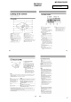
MZ-R500/R500PC SERVICE MANUAL US Model Canadian Model Ver 1.0 Ver 1.0 2001. 2001. 01 06 MZ-R500/R500PC AEP Model UK Model E Model Chinese Model This service manual contains the information on the MZ-R500 (9-873-054-11). MZ-R500 Photo: MZ-R500 US and foreign patents licensed from Dolby Laboratories Licensing Corporation.
MZ-R500/R500PC Battery operation time Battery life1) LR6 (SG) alkaline dry battery3) Recording4) Playback (Unit: approx.hours) (EIAJ2)) Normal LP2 LP4 7.5 10 13.5 36 42 48 The battery life may be shorter due to operating conditions, the temperature of the location, and varieties of batteries. 2) Measured in accordance with the EIAJ (Electronic Industries Association of Japan) standard. 3) When using a Sony LR6 (SG) “STAMINA” alkaline dry battery (produced in Japan).
MZ-R500/R500PC TABLE OF CONTENTS 1. SERVICING NOTE ......................................................... 4 2. GENERAL Looking at the Controls ...................................................... 5 Record an MD ..................................................................... 5 Playing an MD right away .................................................. 6 3. DISASSEMBLY 3-1. Case (Lower) Assy .............................................................. 7 3-2. Case (Upper) Assy ..................
MZ-R500/R500PC SECTION 1 SERVICING NOTE NOTES ON HANDLING THE OPTICAL PICK-UP BLOCK OR BASE UNIT The laser diode in the optical pick-up block may suffer electrostatic break-down because of the potential difference generated by the charged electrostatic load, etc. on clothing and the human body. During repair, pay attention to electrostatic break-down and also use the procedure in the printed matter which is included in the repair parts. The flexible board is easily damaged and should be handled with care.
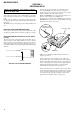
MZ-R500/R500PC SECTION 2 GENERAL This section is extracted from instruction manual.
MZ-R500/R500PC 6
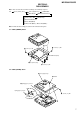
MZ-R500/R500PC SECTION 3 DISASSEMBLY Note : This set can be disassemble according to the following sequence. Set Case (Lower) Assy Case (Upper) Assy Main Board Service Assy, OP LCD Module MD Mechanism Deck Holder Assy Motor Flexible Board Motor, DC (M602) "Motor, DC (M601)"," Motor, DC (M603)" Note : Follow the disassembly procedure in the numerical order given. 3-1. CASE (LOWER) ASSY 4 claw 3 screws (1.7), MI 1 screw (1.7), MI knob (hold) 5 6 case(lower) assy 2 screw (1.7), MI 3-2.
MZ-R500/R500PC 3-3. LCD MODULE 2 screws (1.7x3), tapping 1 screws (1.7x3), tapping 4 LCD module 3 case (upper) assy 3-4. MAIN BOARD 4 screws (M1.4x2), toothed lock 2 Remove the solders 7 CN501 3 screws (M1.4x2), toothed lock qa Remove the solder 6 1 CN701 8 MAIN board qs terminal (-), battery 5 screw (M1.
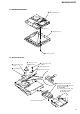
MZ-R500/R500PC 3-5. MD MECHANISM DECK 3 MD mechanism deck boss 2 chassis assy, set 1 screws (1.7), MI 3-6. SERVICE ASSY, OP 1 washer (0.8 - 2.5) 3 precision pan screw (M1.4) 2 gear (SA) 5 precision pan screw (M1.4) 6 spring, thrust detent 4 rack spring (S) 8 Pull off the lead screw. 7 9 Opening the over write head toward the direction A, remove the OP Service assy toward the direction B. Note: Do not open the entire assy forcibly, when opening the over write head.
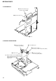
MZ-R500/R500PC 3-7. HOLDER ASSY 4 Remove the holder assy to direction of the arrow B. 1 Open the holder assy. A 2 B 3 boss 3-8. MOTOR FLEXIBLE BOARD 1 Remove four solders of DC motor (sled) (M602). 5 motor flexible board 2 Remove two solders of DC motor (over write head up/down) (M603). 4 adhesive sheet Note: Align a circular hole in the stripping paper with a circular hole in the DC motor (sled), when mounting the motor flexible board. 10 3 Remove four solders of DC motor (spindle) (M601).
MZ-R500/R500PC 3-9. MOTOR, DC (M602) 1 Remove four solders of motor flexible board. 2 washer (0.8 - 2.5) 4 two precision pan screws (M1.4) 3 gear (SA) 5 DC motor (sled) (M602) 3-10. “MOTOR, DC (M601)”, “MOTOR, DC (M603)” 1 Remove six solders of motor flexible board. qs DC motor (over write head up/down) (M603) Note: Press-fit the gear (HA) up to the position of the DC motor (over write head up/down) (M603) as shown below. gear (HA) 6 two precision pan screws (M1.4) 4 three precision pan screws (M1.
MZ-R500/R500PC SECTION 4 TEST MODE 4-1. Outline 4-3. Operation in Setting the Test Mode • This set provides the Overall adjustment mode that allows CD and MO discs to be automatically adjusted when in the test mode. In this overall adjustment mode, the disc is discriminate between CD and MO, and each adjustment is automatically executed in order. If a fault is found, the system displays its location. Also, the manual mode allows each individual adjustment to be automatically adjusted.
MZ-R500/R500PC 4-5. Configuration of Test Mode Major item switching Test mode (Display Check Mode) Press the > or VOL+ key Manual Mode Press the x key x key Servo Adjustment Press the . or VOL– Audio Adjustment Power Supply Adjustment Medium item switching OP Alignment Adjustment N key x key VOL – key: 100th Place of item number decrease. VOL + key: 10th Place of item number increase. VOL – key: 10th Place of item number decrease.
MZ-R500/R500PC 5. The display changes a shown below each time the [ENTER] key on the set is pressed. • Address & Adjusted Value Display This set LCD display 0 11 3A4S1D adjustment value address • Jitter Value & Adjusted Value Display This set LCD display item number 4-8.
MZ-R500/R500PC • Description of Error Indication Codes Problem No error Servo system error TOC error Power supply system error Offset system error Indication code Meaning of code Simple display Description 00 No error --- No error 01 Illegal access target address was specified Adrs Attempt to access an abnormal address 02 High temperature Temp High temperature 03 Focus error Fcus Disordered focus 04 Spindle error Spdl Abnormal rotation of disc 11 TOC error TOC Faulty TOC cont
MZ-R500/R500PC 4-10. Sound Skip Check Result Display Mode • Cause of Sound Skip Error This set can display the count of errors that occurred during the recording/playing for checking. Cause of error EIB • Setting method of sound skip check result display mode 1. Set the test mode (see page 12). 2. Press the N key or [T.MARK] + [PLAY] keys, and the playing or recording sound skip result display mode becomes active respectively where the LCD displays the following.
MZ-R500/R500PC 4. When all the keys on the set and on the remote commander are considered as OK, the following displays are shown for 4 seconds. Example1: When the keys on the set are considered as OK: This set LCD display 8 8 8 RMC OK 5. When all keys were checked or if the upper panel is opened, the key check mode quits and the test mode (display check mode) comes back.
MZ-R500/R500PC SECTION 5 ELECTRICAL ADJUSTMENTS 5-1. Outline • In this set, automatic adjustment of CD and MO can be performed by entering the test mode (see page 12). However, before starting automatic adjustment, the memory clear, power supply adjustment, and laser power check must be performed in the manual mode. • A key having no particular description in the text, indicates a set key. • For the LCD display, the LCD display on the set is shown. • Setting method of NV reset 1.
MZ-R500/R500PC 3) Press the X key to write the adjusted value. 4) Select the manual mode of the test mode, and set item number 862 (see page 13). This set LCD display • Setting method of power supply manual adjustment 1. Make sure that the power supply voltage is 3V. 2. Set the test mode (see page 12). 3. Press the . or [VOL--] key to activate the overall adjustment mode.
MZ-R500/R500PC 2. Connect a digital voltmeter to the TP902 (VC) on the MAIN board, and adjust [VOL +] key (voltage up) or [VOL --] key (voltage down) so that the voltage becomes 2.75 ± 0.01 V. digital voltmeter 3. Adjust with [VOL +], [VOL --] key so that the adjusted value (hexadecimal value) becomes the ambient temperature. (Initial value: 14h = 20 °C, Adjusting range: 80h to 7fh (–128 °C to +127 °C) This set LCD display MAIN board TP902(VC) TP910(GND) 0 14 3.
MZ-R500/R500PC 8. Press the N key, and set the laser CD read adjustment mode (item number 012). 5-8. Overall Adjustment Mode • Configuration of overall adjustment This set LCD display Overall adjustment mode (Title display) 0 1 2 HrefPw N key Protect switch ON 9. Press the [ENTER] key and set the address & adjusted value display (see page 14). .
MZ-R500/R500PC • Overall Adjustment Mode (Title Display) This set LCD display 0 0 0Assy : (Disc mark) At end power supply adjustment:Outside lit At end of electrical offset adj.:inside lit Note:On the set having microcomputer version 1.000,the disc mark is displayed on the set LCD only. : Left side = MO overall adjustment information F : MO overall adjustment completed 1 : Manual adjustment exists(overall adj.
MZ-R500/R500PC • Overall CD and MO adjustment items 1. Overall CD adjustment items Item No. 312 313 CD electrical offset adjustment 321 CD tracking error gain adjustment 328 CD TWPP gain adjustment 332 CD ABCD gain adjustment 344 CD focus gain adjustment 345 CD tracking gain adjustment 522 • Resume Clear Setting Method 1. Select the manual mode of the test mode, and set item number 043 (see page 13).
MZ-R500/R500PC 4. Write specific modified data. For a version where there is no need for writing specific modified data, the power should be turned off once. 9. Press the X key. (0D58 is blinking) This set LCD display • Modified Data Writing Method (version 1.000) 1. Select the manual mode of the test mode, and set item number 022 (see page 13). 0 2 3 0D581E 1E: Adjusted value This set LCD display 10. Press the [VOL+] key once to change the blinking portion to 0D59.
MZ-R500/R500PC 20. Adjust with the [VOL+] key (adjusted value up) or [VOL--] key (adjusted value down) so that the adjusted value becomes 20. This set LCD display 31. Press the x key. (00 is blinking) 32. Adjust with the [VOL+] key (adjusted value up) or [VOL--] key (adjusted value down) so that the adjusted value becomes 04. This set LCD display 0 23 0D5F20 20: Adjusted value 21. Press the X key. (0D5F is blinking) 22. Press the [VOL+] key once to change the blinking portion to 0D60.
MZ-R500/R500PC • Modified Data Writing Method (version 1.100) 1. Select the manual mode of the test mode, and set item number 022 (see page 13). This set LCD display 0 2 2 PatClr 2. Press the [ENTER] key and set the address & adjusted value display (see page 14). This set LCD display 11. Adjust with the [VOL+] key (adjusted value up) or [VOL--] key (adjusted value down) so that the adjusted value becomes AA. This set LCD display 0 2 30D5DAA AA: Adjusted value 12. Press the X key. (0D5D is blinking) 13.
MZ-R500/R500PC 23. Adjust with the [VOL+] key (adjusted value up) or [VOL--] key (adjusted value down) so that the adjusted value becomes F4. This set LCD display 35. Adjust with the [VOL+] key (adjusted value up) or [VOL--] key (adjusted value down) so that the adjusted value becomes 80. This set LCD display 0 230D6880 0 2 30D64F4 F4: Adjusted value 24. Press the X key. (0D64 is blinking) 25. Press the [VOL+] key once to change the blinking portion to 0D65.
MZ-R500/R500PC 47. Adjust with the [VOL+] key (adjusted value up) or [VOL--] key (adjusted value down) so that the adjusted value becomes 1C. This set LCD display 59. Adjust with the [VOL+] key (adjusted value up) or [VOL--] key (adjusted value down) so that the adjusted value becomes D3. This set LCD display 0 2 30D73D3 0 230D6D1C 1C: Adjusted value 48. Press the X key. (0D6D is blinking) 49. Press the [VOL+] key once to change the blinking portion to 0D6E.
MZ-R500/R500PC 71. Adjust with the [VOL+] key (adjusted value up) or [VOL--] key (adjusted value down) so that the adjusted value becomes 03. This set LCD display 82. Press the [ENTER] key and set the address & adjusted value display (see page 14). This set LCD display 0 23 0 2 30D7603 03: Adjusted value 72. Press the X key. (0D76 is blinking) 73. Press the [VOL+] key to change the blinking portion to 0D78. This set LCD display 83. Press the X key to write the modified data.
MZ-R500/R500PC SECTION 6 DIAGRAMS 6-1. IC PIN FUNCTION DESCRIPTION • IC501 SN761057DBT (RF AMP, FOCUS/TRACKING ERROR AMP) Pin No.
MZ-R500/R500PC • IC801 CXD2671-204GA (SYSTEM CONTROLLER, DIGITAL SIGNAL PROCESSOR, 16M BIT D-RAM) Pin No. Pin Name I/O Description 1 PAUSE KEY I Set key input terminal (X key input) 2 (MIC SENSE) O Control signal output to the microphone amp “H”: HIGH, “L”: LOW, normally: “H” Not used (open) 3 4, 5 XTEST NC I O Input terminal for the test mode set up Not used (open) 6 7 MCUVDD0 MIFVSS3 — — Power supply terminal (for microcomputer block) (+1.
MZ-R500/R500PC Pin No. 52 Pin Name AVD2 I/O — Description Power supply terminal (for the analog) (+2.4 V) 53 54 AVS2 ADRB — I Ground terminal (for the analog) A/D converter the lower limit voltage input (fixed at “L” in this set) 55 56 SE TE I I 57 58 DCHG APC — I Connecting analog power supply of the low impedance (fixed at “H” in this set) Error signal input for the laser automatic power control Not used (fixed at “H”) 59 60 DSPVDD0 DSPVSS0 — — Power supply terminal (for DSP block) (+1.
MZ-R500/R500PC Pin No. Pin Name I/O Description Sled motor drive signal output (W) to the motor driver (IC701)/drive control signal 99 SLDW O 100 SLCU I output (2+) Spindle motor drive comparison signal input (U) from the motor driver (IC701) 101 102 SLCV SLCW I I Spindle motor drive comparison signal input (V) from the motor driver (IC701) Spindle motor drive comparison signal input (W) from the motor driver (IC701) 103 104 DIFVDD1 DIFVSS1 — — Power supply terminal (for DSP I/F) (+2.
MZ-R500/R500PC Pin No.
MZ-R500/R500PC Pin No.
MZ-R500/R500PC 6-2.
MZ-R500/R500PC 6-3.
MZ-R500/R500PC 6-4.
MZ-R500/R500PC Common note on Printed Wiring Board: • Y : parts extracted from the conductor side. • : Pattern from the side which enables seeing. (The other layer’s patterns are not indicated.) Caution: Pattern face side: (Side B) Parts face side: (Side A) Common note on Schematic Diagram: • All capacitors are in µF unless otherwise noted. pF: µµF 50 WV or less are not indicated except for electrolytics and tantalums. • All resistors are in Ω and 1/4 W or less unless otherwise specified.
MZ-R500/R500PC 6-5. PRINTED WIRING BOARD — MAIN SECTION — • Refer to page 39 for Note.
MZ-R500/R500PC 14 13 12 11 10 9 8 7 6 5 4 3 2 1 A • Semiconductor Location (SIDE B) D101 C107 MAIN BOARD (SIDE B) TP319 (HP GND) TP101 (HP L) J302 AP302 R111 R110 R105 AP303 C830 AP722 C828 TP828 AP841 AP831 AP833 AP842 AP845 AP844 AP840 AP864 AP839 AP862 AP843 AP834 AP853 AP836 AP727 AP850 AP813 AP805 C610 AP814 C821 L802 AP809 AP810 AP808 C609 H 1 I 20 IC601 C620 C706 C601 C602 C619 C617 25 28 29 5 50 R610 4 R611 Q603 35 R604 C611 R605 C612
MZ-R500/R500PC 6-6. SCHEMATIC DIAGRAM — MAIN SECTION (1/3) — • Refer to page 39 for Waveforms. Refer to page 45 for IC Block Diagrams. Refer to page 39 for Note.
MZ-R500/R500PC 6-7. SCHEMATIC DIAGRAM — MAIN SECTION (2/3) — • Refer to page 39 for Waveforms. Refer to page 47 for IC Block Diagrams. Refer to page 39 for Note.
MZ-R500/R500PC 6-8. SCHEMATIC DIAGRAM — MAIN SECTION (3/3) — • Refer to page 48 for IC Block Diagrams. Refer to page 39 for Note.
MZ-R500/R500PC • IC BLOCK DIAGRAMS IC501 SN761057DBT 44 ADIP-IN 43 S-MON A+B+C+D I+J NPP TON CSL Aw+Dw TON Peak TON Botm ADIP TE TE 1 REXT 2 Wpp LPF 3 VREF 4 C 5 D 6 TE TWpp PK/BTM Aw CSLO VREF075 A-C D-C Malfa Mij AwBPF Dw DwBPF S-MONITOR TEMP D-C 7 Tpp/Wpp RF Iy 8 Ix 9 FE Jx 10 Jy 11 ABCD A 12 A-C 13 PEAK/BOTM B 14 TON-C CIG CDN PD-I PD-NI PD-O 15 16 17 18 19 20 ADIP 21 DVDD 22 42 41 40 39 38 37 36 35 34 33 32 31 30 29 28 FE ABCD OFC-1 OFC-2 AVCC PS LP EQ AGND RF OUT CCSL2 VC VREF075 P
MZ-R500/R500PC VM3 RO3 PGND3 FO3 VM34 RO4 PGND4 FO4 40 39 CPBO 42 41 CPAO CPBIP CPBIM SC111257FCR2 CPAIP CPAIM IC701 38 37 36 35 34 33 32 31 30 29 – + 28 VM4 VC – + VC VG VG PRE DRIVER PRE DRIVER VG VC PGNDW 43 VC VC H-BRIDGE CONTROL WO 44 PRE DRIVER VMVW 45 H-BRIDGE CONTROL VO 46 27 RI4 26 FI4 PGNDUV 47 25 RI3 24 FI3 VG UO 48 23 VG VC VMU 49 22 VC VC GND2 50 CPWI 51 CPVI 52 – + CPUI 53 – + COM 54 21 GND1 BIAS – + 20 PWM24 19 FI1 18 RI1 17 FI2 16 RI2
MZ-R500/R500PC VRECIN2 VG HB PGND3 HA 39 38 37 36 35 34 33 VG3 VG OUTPUT SW VGC VC2 VC EFM PRE DRIVER CONTROL 28 C1H 27 C1L CHARGE PUMP 1 CHARGE PUMP 2 26 VC2 VREF BUFFER VG3 DC IN 29 VC2 VG VG3 VC HI-BRIDGE PRE DRIVER CHARGE MONITOR X2/X4 BATM 44 32 31 30 OUTPUT SW VC VG DC IN VB 43 VG2 VG2 OUTB 40 C2L PGND2 41 C2H PGND2 42 VG3 OUTA XPC18A22FCR2 VRECIN1 IC601 25 VREF 24 CVREF CONTROL 23 GND CHARGE CONTROL CHGSW 45 22 DW BT 21 DW TP DC IN 46 47 48 49 VC
MZ-R500/R500PC IC301 AK5354VT 16 PDN CONTROL REGISTER I/F 15 CSN 14 CCLK 13 CDTI 12 LRCK 11 MCLK CLOCK DIVIDER LIN1 1 10 BCLK IPGA ADC HPF AUDIO I/F CONTROLLER RIN1 2 LIN2 3 RIN2 4 VCON VCON 5 AGND 6 VA 7 VA VD 8 VD GND VREF IN 18 17 16 15 14 13 PW SW MT SW BST SW BEEP STB MUTE BEEP TA2131FL BST SW IC302 V REF 12 VREF 11 LPF1 TCMT 19 VCC 20 ADD IN R 21 10 NF1 BST1 IN L 22 9 LPF2 PW A OUTB BEEP 23 PW B BST2 8 NF2 7 BST OUTA BEEP 24 48 1 2 3 4 5 6 +B OUT
MZ-R500/R500PC SECTION 7 EXPLODED VIEWS NOTE: • The mechanical parts with no reference number in the exploded views are not supplied. • Items marked “*” are not stocked since they are seldom required for routine service. Some delay should be anticipated when ordering these items. • Abbreviation AR : Argentine model CH : Chinese model EE : East European model FR : French model TW : Taiwan model • -XX and -X mean standardized parts, so they may have some difference from the original one.
MZ-R500/R500PC 7-2. CASE (UPPER) SECTION 52 51 53 54 61 55 62 58 56 60 57 58 58 59 Ref. No. 51 51 51 51 51 51 52 52 52 53 50 Part No. Description Remark 3-225-619-01 3-225-619-11 3-225-619-21 3-225-619-31 CASE (UPPER) (SILVER)...(SILVER) CASE (UPPER) (BLUE)...(BLUE) CASE (UPPER) (BLACK)...(BLACK) CASE (UPPER) (DARK BLUE)... (DARK BLUE) 3-225-619-41 CASE (UPPER) (RED)...(RED) 3-225-619-51 CASE (UPPER) (YELLOW)...(YELLOW) 3-225-622-01 WINDOW (LCD) (BLUE)...
MZ-R500/R500PC 7-3. CHASSIS SECTION MT-MZR500-172 102 101 114 111 110 113 112 109 103 104 108 106 105 107 105 Ref. No. Part No. Description Remark 101 102 103 * 104 * 104 X-3379-969-1 3-318-382-01 4-218-233-11 A-3021-481-A A-3021-482-A CHASSIS ASSY SCREW (1.7X3), TAPPING SCREW (1.7), MI MAIN BOARD, COMPLETE (US) MAIN BOARD, COMPLETE (CND) * 104 105 106 A-3323-653-A MAIN BOARD, COMPLETE (EXCEPT US,CND) 3-335-797-01 SCREW (M1.4X2), TOOTHED LOCK 3-225-630-01 TERMINAL (+), BATTERY Ref. No.
MZ-R500/R500PC 7-4. MD MECHANISM DECK SECTION (MT-MZR500-172) 151 167 169 170 168 152 155 153 168 156 B B A A 154 158 173 M603 157 165 171 172 160 162 M602 161 M601 165 153 173 153 163 159 Ref. No. 164 159 Part No. Description 151 152 153 154 155 X-3379-515-1 3-224-779-01 4-963-883-42 X-3379-514-1 4-222-218-01 HOLDER ASSY SPRING, THRUST DETENT SCREW (M1.
MZ-R500/R500PC SECTION 8 ELECTRICAL PARTS LIST NOTE: • Due to standardization, replacements in the parts list may be different from the parts specified in the diagrams or the components used on the set. • -XX and -X mean standardized parts, so they may have some difference from the original one. • RESISTORS All resistors are in ohms. METAL:Metal-film resistor. METAL OXIDE: Metal oxide-film resistor.
MZ-R500/R500PC MAIN Ref. No. Part No. Description Part No. Description C705 C706 C707 C708 C709 1-135-211-11 1-135-211-11 1-104-912-11 1-119-749-11 1-104-912-11 TANTAL. CHIP TANTAL. CHIP TANTAL. CHIP TANTAL. CHIP TANTAL. CHIP 6.8uF 6.8uF 3.3uF 33uF 3.3uF 20% 20% 20% 20% 20% 6.3V 6.3V 6.3V 4V 6.3V C910 C911 C912 C913 C914 1-115-169-11 1-164-941-11 1-115-169-11 1-119-749-11 1-128-964-11 TANTALUM CERAMIC CHIP TANTALUM TANTAL. CHIP TANTAL. CHIP 10uF 0.
MZ-R500/R500PC MAIN Ref. No. FB801 FB802 FB803 FB804 FB806 Part No. Description 1-414-226-21 1-216-864-11 1-216-864-11 1-216-864-11 1-216-864-11 FERRITE, EMI (SMD) (US,CND) METAL CHIP 0 5% METAL CHIP 0 5% METAL CHIP 0 5% METAL CHIP 0 5% Remark Part No. Description Remark < RESISTOR > 1/16W 1/16W 1/16W 1/16W < IC > R102 R103 R105 R106 R107 1-218-990-11 1-218-967-11 1-218-961-11 1-208-635-11 1-218-963-11 SHORT RES-CHIP RES-CHIP RES-CHIP RES-CHIP 0 15K 4.7K 10 6.
MZ-R500/R500PC MAIN Ref. No. Part No. Description R801 R804 R805 R806 R807 1-218-990-11 1-218-990-11 1-218-981-11 1-208-927-11 1-208-927-11 SHORT SHORT RES-CHIP METAL CHIP METAL CHIP 0 0 220K 47K 47K Remark 5% 0.5% 0.5% 1/16W 1/16W 1/16W R808 R809 R810 R811 R812 1-218-959-11 1-218-959-11 1-218-949-11 1-208-635-11 1-218-965-11 RES-CHIP RES-CHIP RES-CHIP RES-CHIP RES-CHIP 3.3K 3.
MZ-R500/R500PC Ref. No. Part No.
MZ-R500/R500PC REVISION HISTORY Clicking the version allows you to jump to the revised page. Also, clicking the version at the upper right on the revised page allows you to jump to the next revised page. Ver. 1.0 58 Date 2001. 06 Description of Revision New (The MZ-R500PC is added.