MZ-N1 SERVICE MANUAL AEP Model UK Model E Model Ver 1.0 2002. 01 US and foreign patents licensed from Dolby Laboratories. • OpenMG, “MagicGate”, “MagicGate Memory Stick”, “Memory Stick”, VAIO,MusicClip and their logos are trademarks of Sony Corporation. • “WALKMAN” is a trademark of Sony Corporation. • Microsoft,Windows,Windows NT and Windows Media are trademarks or registered trademarks of Microsoft Corporation in the United States and/or other countries.
MZ-N1 Modulation system EFM (Eight to Four teen Modula tion) Frequency response 20 to 20, 000 Hz ± 3 dB Wow and Flutter Below measurable limit Inputs 1) MIC : stereo mini-ja ck (minimum inpu t leve l 0.
MZ-N1 CAUTION Use of controls or adjustments or performance of procedures other than those specified herein may result in hazardous radiation exposure. TABLE OF CONTENTS 1. SERVICING NOTES ............................................... 4 2. GENERAL ................................................................... 5 On power sources 3. DISASSEMBLY • Use house curre nt, nikel metal hyd ride rechargeable battery, LR6 (S G) battery, or car battery.
MZ-N1 SECTION 1 SERVICING NOTES NOTES ON HANDLING THE OPTICAL PICK-UP BLOCK OR BASE UNIT • Replacement of CXD2677-202GA (IC801) used in this set requires a special tool. The laser diode in the optical pick-up block may suffer electrostatic break-down because of the potential difference generated by the charged electrostatic load, etc. on clothing and the human body.
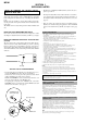
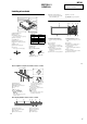
MZ-N1 SECTION 2 GENERAL This section is extracted from instruction manual. Looking at controls The recorder P MIC (PLUG IN POWER) jack There is a tactile dot beside the MIC (PLUG IN POWER) jack. J 1 2 3 4 5 Q REC (record) switch R i (headphones/earphones)/LINE OUT jack qa qs The display window of the recorder qd 1 2 3 4 5 6 qf 6 qg 7 qh 8 qj 9 qk A END SEARCH button B Display window C VOLUME +/– buttons • Other operations The VOLUME + button has a tactile dot.
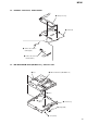
MZ-N1 SECTION 3 DISASSEMBLY • This set can be disassembled in the order shown below. 3-1. DISASSEMBLY FLOW SET 3-2. BOTTOM PANEL ASSY (Page 7) 3-3. UPPER PANEL SECTION (Page 7) 3-4. LCD MODULE, UPPER PANEL ASSY (Page 8) 3-5. MAIN BOARD SECTION (Page 8) 3-6. BATTERY CASE ASSY, MAIN BOARD (Page 9) 3-7. MD MECHANISM DECK (MT-MZN1-171), CHASSIS ASSY (Page 9) 3-8. OP SERVICE ASSY (LCX-5R) (Page 10) 3-9. HOLDER ASSY (Page 11) 6 3-10. DC MOTOR (SLED) (M602) (Page 11) 3-11.
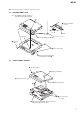
MZ-N1 Note: Follow the disassembly procedure in the numerical order given. 3-2. BOTTOM PANEL ASSY Note : On installation, adjust the position of both switch (S801) and knob (hold). S801 3 Remove the battery case lid. 1 Open the battery case lid. 2 claw knob (hold) 4 Close the battery terminal (plus). 5 two screws (M1.4) 5 three screws (M1.4) A 3-3. 6 Remove the bottom panel assy in the direction of arrow A. UPPER PANEL SECTION 3 two screws (M1.
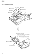
MZ-N1 3-4. LCD MODULE, UPPER PANEL ASSY 1 four screws (1.7) 2 Remove the LCD module in the direction of the arrow. 3 upper panel section 3-5. MAIN BOARD SECTION 6 flexible board (optical pick-up) (CN501) 5 7 holder (terminal) 1 Remove two solders of the flexible board (over write head). 8 main board section 3 four screws (M1.4) 4 screw (M1.
MZ-N1 3-6. BATTERY CASE ASSY, MAIN BOARD 2 battery case assy 3 main board 1 Remove the solder of terminal (plus). 1 Remove the solder of terminal (minus). 3-7. MD MECHANISM DECK (MT-MZN1-171), CHASSIS ASSY 2 boss 3 MD mechanism deck (MT-MZN1-171) 2 boss 1 screw (M1.4) 5 chassis assy 4 spring (POP) 1 screw (M1.
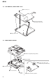
MZ-N1 3-8. OP SERVICE ASSY (LCX-5R) 2 gear (SA) 5 screw (M1.4) 1 washer (0.8-2.5) 6 thrust detent spring 3 screw (M1.4) 8 Pull off lead screw. 4 rack spring 7 9 Opening the over write head toward the direction A, remove the OP service assy (LCX-5R) toward the direction B. B Note: Do not open the entire assy forcibly, when opening the over write head.
MZ-N1 3-9. HOLDER ASSY 5 Remove the holder assy in the direction of arrow D. B 2 Push the convex portion toward the direction B and open the holder assy toward the direction A to erect uprightly. 1 Open the holder assy. C 3 Remove the concave portion in the direction of arrow C. A D 4 convex portion 3-10. DC MOTOR (SLED) (M602) 2 washer (0.8-2.5) 3 gear (SA) 4 two screws (M1.4) 1 Remove six solders of the motor flexible board.
MZ-N1 3-11. DC SSM18B MOTOR (SPINDLE) (M601), DC MOTOR (OVER WRITE HEAD UP/DOWN) (M603) 1 Remove six solders of the motor flexible board. Note : Press-fit the gear (HA) up to the position of the DC motor (over write head up/down) (M603) as shown below. qa DC motor (over write head up/down) (M603) gear (HA) 6 two screws (M1.4) 2.65mm qs gear chassis assy 4 three screws (M1.4) 5 DC SSM18B motor (spindle) (M601) gear chassis assy 9 screw (M1.2 × 1.
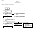
MZ-N1 SECTION 4 TEST MODE Outline Operation in Setting the Test Mode • This set provides the Overall adjustment mode that allows CD and MO discs to be automatically adjusted when in the test mode. In this overall adjustment mode, the disc is discriminate between CD and MO, and each adjustment is automatically executed in order. If a fault is found, the system displays its location. Also, the manual mode allows each individual adjustment to be automatically adjusted.
MZ-N1 Configuration of Test Mode [Test Mode $Display Check Mode%] Press the > or [VOLUME +] key [Manual Mode] Press the x/CHG key [Servo Adjustment] [Audio Adjustment] [Power Supply Adjustment] [OP Alignment Adjustment] Press the .
MZ-N1 5. The display changes a shown below each time the jog dial (down) is turned or the [DISPLAY] key on the remote commander is pressed.
MZ-N1 • Description of error indication codes Problem Indication code No error Servo system error TOC error Power supply system error Offset system error Meaning of code No error 01 Illegal access target Adrs address was specified Attempt to access an abnormal address No error 02 High temperature Temp High temperature detected 03 Focus error Fcus Disordered focus or can not read an address 04 Spindle error Spdl Abnormal rotation of disc 11 TOC error TOC Faulty TOC contents 12 Da
MZ-N1 Sound Skip Check Result Display Mode Jog and Key Check Mode This set can display the count of errors that occurred during the recording/playing for checking. This set can check if the set and remote commander function normally. • Setting method of sound skip check result display mode 1. Set the test mode (see page 13). 2. Press the N key or [REC] key, and the playing or recording sound skip result display mode becomes active respectively where the LCD displays the following.
MZ-N1 Example1: When the > key on the set is pressed: Remote commander LCD display 000 FF ** **: AD value of the remote commander key (hexadecimal 00 to FF) Example2: When the N > key on the remote commander is pressed: Remote commander LCD display 000 rPLAY ** **: AD value of the remote commander key (hexadecimal 00 to FF) 4. When all the keys on the set and on the remote commander are considered as OK, the following displays are shown for 4 seconds.
MZ-N1 SECTION 5 ELECTRICAL ADJUSTMENTS Outline NV Reset • In this set, automatic adjustment of CD and MO can be performed by entering the test mode. However, before starting automatic adjustment, the memory clear, power supply adjustment, and laser power check must be performed in the manual mode. • A key having no particular description in the text, indicates a set key. • For the LCD display, the LCD on the remote commander is shown, but the contents of LCD display on the set are same.
MZ-N1 2. NV adjusted values modifying procedure 1) Select manual mode of the test mode, and set item number 336 (see page 14). Remote commander LCD display 336 AbcdGn ** **: Adjusted value 2) Adjust with the [VOLUME +] key (adjusted value up) or [VOLUME --] key (adjusted value down) so that the adjusted value becomes 8. 3) Press the X key to write the adjusted value. 4) Select manual mode of the test mode, and set item number 149 (see page 14). 5) Press the > key to set item number 151.
MZ-N1 38) Select manual mode of the test mode, and set item number 873 (see page 14). 7) Select manual mode of the test mode, and set item number 866 (see page 14). Remote commander LCD display Remote commander LCD display 873 V6 num ** 866 V3 dat ** **: Adjusted value 39) Adjust with the [VOLUME +] key (adjusted value up) or [VOLUME --] key (adjusted value down) so that the adjusted value becomes BB. 40) Press the X key to write the adjusted value.
MZ-N1 25) Select manual mode of the test mode, and set item number 874 (see page 14). • Adjustment method of Vc PWM Duty (H) (item number: 763) Remote commander LCD display Remote commander LCD display 763 VchPWM 874 V6 dat ** ** **: Adjusted value **: Adjusted value 26) Adjust with the [VOLUME +] key (adjusted value up) or [VOLUME --] key (adjusted value down) so that the adjusted value becomes 05. 27) Press the X key to write the adjusted value.
MZ-N1 • Adjustment method of Vrec PWM Duty (L) (item number: 766) Remote commander LCD display 766 RECpwL ** Temperature Correction • Adjustment method of temperature correction 1. Select the manual mode of test mode, and set the item number 015 (see page 14). Remote commander LCD display **: Adjusted value 1. Connect a digital voltmeter to the AP611 (VREC) on the MAIN board, and adjust [VOLUME +] key (voltage up) or [VOLUME + 0.025 --] key (voltage down) so that the voltage becomes 1.08 – 0.005 V.
MZ-N1 10. Press the N key, and set the laser MO write adjustment mode (item number 013). Remote commander LCD display 013 WritPw ** 11. Check that the laser power meter reading is 4.95 ± 0.50 mW. 12. Check that the voltage both ends (TP (+) and TP (–)) of resistor R521 at this time is below 80 mV. 13. Press the x/CHG key to quit the manual mode, and activate the test mode (display check mode).
MZ-N1 • Overall adjustment mode (title display) Overall Adjustment Mode • Configuration of overall adjustment mode Remote commander LCD display Overall adjustment mode . key (Title display) N key Protect switch ON 000 Assy** CD overall adjusting All item OK NG item exists or x/CHG key CD overall adjustment NG x/CHG key x/CHG key Protect switch OFF > key CD overall adjustment OK Note: Adjust the CD first, when performing adjustment.
MZ-N1 4. In case of CD overall adjustment NG, reset the NV (see page 19), then readjust from the temperature correction (see page 21). Remote commander LCD display 000 *** NG 2. MO overall adjustment items Item No. 112 113 114 Description MO electrical offset adjustment 118 **: NG item number. 5. If OK through the CD overall adjustments, then perform MO overall adjustments. Remote commander LCD display 000 CD OK 6.
MZ-N1 Rewriting the Patch Data at Replacement of Main Board or Nonvolatile Memory (IC802) This set requires the patch data in the nonvolatile memory (IC802) to be rewritten using the application, when the MAIN board or nonvolatile memory (IC802) was replaced. Caution: The application that meets the microcomputer version in this set must be used when rewriting the patch data. Rewriting the patch data using the application not suitable for the microcomputer version could cause the set to malfunction.
MZ-N1 5. Confirm that the model and version indicated on the title bar coincide with the codes displayed in the Device Name block and the Version block in the window. 6. Click the [Write + Verify] button. The patch data writing and the verify processing will be executed automatically in the following order: 1) Writing to patch area (front area) 2) Writing to patch area (reverse area) 3) Verifying patch area (front area) 4) Verifying patch area (reverse area) 7.
MZ-N1 8. Click the [Usb Disconnect] button. 10. Disconnect the USB cable from the personal computer and the USB cradle. 11. Remove the set from the USB cradle. 9. Confirm that the window becomes as shown below where the [Write + Verify] button and [Read] button are inactive.
MZ-N1 SECTION 6 DIAGRAMS BLOCK DIAGRAM – SERVO/USB Section – OVER WRITE HEAD DRIVE IC601 (1/2) HR601 OVER WRITE HEAD 33 M603 OVER WRITE HEAD UP/DOWN RF AMP, FOCUS/TRACKING ERROR AMP IC501 41 38 M HB CLK OUTA OUTB – + B – + – + C C D RF OUT PEAK /BOTM RF AMP, FOCUS/ TRACKING ERROR AMP 13 D-C 7 18 PD-NI 163 RFI 29 28 169 PEAK 170 BOTM 41 171 ABCD 42 172 FE TE 1 ADIP IN 44 181 TE PEAK BOTM FE TPP/WPP ADFG 21 APC 19 LD-A AUTOMATIC POWER CONTROL Q501 20 PD-O XRST 25 S-MONITE
MZ-N1 6-2.
MZ-N1 6-3.
MZ-N1 6-4. NOTE FOR PRINTED WIRING BOARD AND SCHEMATIC DIAGRAMS Note on Printed Wiring Board: • X : parts extracted from the component side. • Y : parts extracted from the conductor side. • : Pattern from the side which enables seeing. (The other layers' patterns are not indicated.) Caution: Pattern face side: (Conductor Side) Parts face side: (Component Side) Parts on the pattern face side seen from the pattern face are indicated. Parts on the parts face side seen from the parts face are indicated.
MZ-N1 6-5.
MZ-N1 6-6. PRINTED WIRING BOARD – MAIN board (Conductor Side) – 1 2 3 :Uses unleaded solder. 4 5 6 7 8 9 10 11 • Semiconductor Location MAIN BOARD (CONDUCTOR SIDE) 1 A U N M602 (SLED) RECHARGEABLE BATTERY NH-14WM 1.2V 1350mAh W V M603 OVER WRITE HEAD UP/DOWN M B U V + X802 K 20 A SWITCH & LCD MODULE J601 DC IN 3V – (CHASSIS) DRY BATTERY SIZE “AA” (IEC DESIGNATION R6) 1PC. 1.
MZ-N1 SCHEMATIC DIAGRAM – MAIN Board (1/4) – • See page 40 for Waveforms. • See page 41 for IC Block Diagrams. B1 (1/4) B2 B3 B4 (Page 38) A0 A1 A2 AP610 A3 HR601 OVER WRITE A4 AP609 HEAD CN501 20P AP611 (VREC) TRK- TRK- Q604 HAT2051T R507 C501 1k 100p TRK+ TRK+ FCSFCS- R501 47k FCS+ FCS+ D1 D2 S1 S2 G1 G2 RF AMP, AGND R503 220k A1 VREF FOCUS/TRACKING ERROR AMP A2 C508 0.1 ADIP C R502 470k D C502 0.022 A3 C527 0.
MZ-N1 SCHEMATIC DIAGRAM – MAIN Board (2/4) – • See page 40 for Waveforms. • See page 41 for IC Block Diagrams. (2/4) D1 A0 D2 VCP VLP A1 D3 A2 D4 A3 D5 D6 TRK- C1 C2 C3 SCW TRK+ A4 D7 C521 0.1 SCV C522 0.1 R915 100 D904 MA2S111 AP911 (VD) R930 1M Q904 2SB1462J S Q907 3LN01SS R925 1M B+ SWITCH FO2 WMF2 RO2 PGND2 VMR2 UO2 VMU2 VO2 WO2 SP PGNDUV2 UI2 VMVW2 VI2 WI2 SCU PGNDW2 R927 1M TR1 RI2 CPUO2 COM2 CPVO2 CPUI2 CPWO2 CPVI2 SMW D1 C902 10 6.
MZ-N1 6-9. SCHEMATIC DIAGRAM – MAIN Board (3/4) – • See page 40 for Waveforms. (3/4) VRP B1 B2 B3 D2 RECHARGEABLE D3 BATTERY IN DETECT D4 SDAT VLP SCLK VCP R865 2.2k D5 R864 1k R866 1k R818 0 C825 10 6.3V C816 0.047 C828 10 6.3V C829 0.1 C815 0.047 F1 R826 2.2k VDP C851 0.1 R814 0 R812 0 S803 R862 1k D803 MA2S728 C845 0.01 R824 2.2k R867 470k D1 R863 1k XJDET XMDET OPDET C817 0.047 R858 1M R825 2.2k DETECT C812 0.
MZ-N1 6-10. SCHEMATIC DIAGRAM – MAIN Board (4/4) – • See page 40 for Waveforms. • See page 41 for IC Block Diagrams. (4/4) C1 (CHASSIS) F1 C213 47 4V (Page 36) C320 10 6.3V C322 47 4V R118 22k 0.5% R106 10k 0.5% R218 22k 0.5% R206 10k 0.5% EEPROM R319 100 IC803 AK6480BL C217 0.1 XBUSY DI RST C212 1 V+1 SK SDO0 OUT1 SDI0 C332 10 6.3V MIC C117 0.1 (PLUG IN POWER) NOISE C218 2200p GND NC SK XBUSY DI RST STBY GV V+2 MIC DC VCC XCS CUT2 OUT2 C841 0.
MZ-N1 • Waveforms 6 IC902 5 (EXT) 1 IC501 1 (TE) qa IC801
MZ-N1 • IC Block Diagrams IC301 AK5354VT-E2 16 PDN LIN1 1 CONTROL REGISTER I/F IPGA RIN1 2 LIN2 3 HPF ADC RIN2 4 15 CSN 14 CCLK 13 CDTI CLOCK DIVIDER VCOM 5 AGND 6 VA 7 12 11 10 9 AUDIO I/F CONTROLLER VD 8 LRCK MCLK BCLK SDTO HP/L MUTE BEEP GA-R IC302 AN17020A-VB 16 15 14 13 HEADPHONE /LINE SWITCH MUTE BEEP – + R-IN 1 12 ROUT 11 GND GND 2 L-IN 3 10 LOUT + – 9 GA-L RIP-F1 4 6 7 8 VCC2 CR 5 RIP-F2 RF2 VCC1 RF1 OUT 1 13 11 10 REG IN1 12 MIC V+1 DC CUT 1 IC30
MZ-N1 IC501 SN761057A 44 ADIP-IN 43 S-MON A+B+C+D I+J NPP TON CSL Aw+Dw TON Peak TON Botm ADIP TE TE 1 REXT 2 Wpp LPF 3 VREF 4 C 5 D 6 TE TWpp PK/BTM Aw CSLO VREF075 A-C D-C Malfa Mij AwBPF Dw DwBPF S-MONITOR TEMP D-C 7 Tpp/Wpp RF Iy 8 Ix 9 FE Jx 10 Jy 11 ABCD A 12 A-C 13 PEAK/BOTM B 14 TON-C CIG CDN PD-NI PD-I PD-O 15 16 17 18 19 20 ADFG 21 DVDD 22 42 42 41 40 39 FE 38 37 36 35 34 AVCC PS 33 32 31 30 29 28 RF CCSL2 VC VREF075 ABCD OFC-C1 OFC-C2 LP EQ AGND PEAK BOTM OF TRK 27 DGND
MZ-N1 VI2 WI2 PGNDW2 WO2 VMVW2 VO2 PGNDUV2 UO2 VMU2 VMR2 RO2 PGND2 FO2 VMF2 IC551 SC111258FCR2 42 41 40 39 38 37 36 35 34 33 32 31 30 29 UI2 43 PWM2 44 3PHASE CONTROL CH2 VC VC VG 3PHASE PRE DRIVER CH2 VC LOW VOLTAGE DETECTOR VC VG H-BRIDGE PRE DRIVER CH2 VC VG CPUO2 45 CPVO2 46 CPWO2 47 VC BIAS H-BRIDGE CONTROL CH2 VC VG 26 COM2 – U+ 25 CPUI2 – V+ 24 CPVI2 – W+ 23 CPWI2 – W+ 20 CPWI1 – + 19 CPVI1 – U+ 18 CPUI1 22 NC 21 GND2 OE 48 GND1 49 VC 50 VG 51 VC VG CPWO1 52
MZ-N1 OUTB VRECIN2 VG HB PGND3 HA 39 38 37 36 35 34 33 VG3 VG OUTPUT SW VC VG DC IN VB 43 BATM 44 CHARGE MONITOR X2/X4 DC IN VG2 VG2 PGND2 40 C2L PGND2 41 C2H OUTA 42 VG3 VRECIN1 IC601 XPC18A22AFCR2 32 31 30 VG2 VC2 VG VG3 OUTPUT SW VC2 VC EFM PRE DRIVER 26 VC2 VREF BUFFER VG3 CONTROL 28 C1H 27 C1L CHARGE PUMP 1 CHARGE PUMP 2 VC HI-BRIDGE PRE DRIVER 29 25 VREF 24 CVREF CONTROL 23 GND CHGSW 45 CHARGE CONTROL 22 DW BT 21 DW TP DC IN RS INP2 INM2 RF2 46 47 48 4
MZ-N1 VA VAFB VDFB VIFFB GND VC VC VC OUT L1 NC PGND1 PGND1 42 41 40 39 38 37 36 35 34 33 32 31 30 29 NC 43 VCO VIF IC901 XPC18A32AFCR2 OUTPUT SW VD 44 VC2 45 OUTPUT SW SERIES PASS REGULATOR VA SERIES PASS REGULATOR VD SERIES PASS REGULATOR VIF 28 L1 OUTPUT SW VC VG + – POWER SWITCH 1 VC VC 26 INM1 VC STEP-UP PRE DRIVER XRST 46 27 RF1 PWM 25 DTC1 OUTPUT SW VC CRST 47 24 DTC2 RSTREF 48 + – BANDGAP REFERENCE 23 RF2 22 INM2 VREF 49 VC VB PWM VB 50 GND 51 21 VDRF
MZ-N1 6-11. IC PIN FUNCTION DESCRIPTION • IC501 SN761057A (RF AMP, FOCUS/TRACKING ERROR AMP) Pin No.
MZ-N1 • IC801 CXD2677-202GA (SYSTEM CONTROLLER, DIGITAL SIGNAL PROCESSOR, 16M BIT D-RAM) Pin No. Pin Name I/O Description 1 NC O Load address strobe signal output terminal for D-RAM Not used 2 NC I Test input terminal for D-RAM Not used 3 to 7 NC O Address signal output terminal for D-RAM Not used 8, 9 NC I/O Two-way data bus terminal for D-RAM Not used 10, 11 DRAMVDD0, 1 — Power supply terminal (for D-RAM) (+2.
MZ-N1 Pin No.
MZ-N1 Pin No.
MZ-N1 Pin No. Pin Name I/O 149 VDIOSC — Description Power supply terminal (for the OSC cell) (+2.2V) 150 OSCI I System clock (45.1584MHz) input terminal 151 OSCO O System clock (45.1584MHz) output terminal 152 VSIOSC I Ground terminal (for the OSC cell) 153 DAVDD — Power supply terminal (for the built-in D/A converter) (+2.
MZ-N1 Pin No. Pin Name I/O Description 195 ADDT I Data input from the external A/D converter 196 LRCK O L/R sampling clock signal (44.1KHz) output to the external A/D converter 197 XBCK O Bit clock signal (2.8224MHz) output to the external A/D converter 198 FS256 O 11.
MZ-N1 Pin No. Pin Name I/O 242 A11 O Address signal output terminal for D-RAM 243 XOE O Output enable signal output terminal for D-RAM 244 XWE O Data write enable signal output terminal for D-RAM 245 TSTDR3 I Test input terminal for D-RAM 246 EVA I EVA/FLASH chip discrimination terminal “L”: FLASH chip, “H”: EVA chip (fixed at “L” in this set) 247 FLASHVDD — Power supply terminal (for the built-in flash memory) (+2.
MZ-N1 SECTION 7 EXPLODED VIEWS NOTE: • -XX and -X mean standardized parts, so they may have some difference from the original one. • Color Indication of Appearance Parts Example: KNOB, BALANCE (WHITE) . . . (RED) ↑ ↑ Parts Color Cabinet's Color • Abbreviation FR : French model HK : Hong Kong model KR : Korean model • Items marked “*” are not stocked since they are seldom required for routine service. Some delay should be anticipated when ordering these items.
MZ-N1 7-2. BOTTOM PANEL SECTION 54 not supplied 55 53 52 51 58 56 57 Ref. No. 51 51 51 51 52 54 Part No. Description Remark X-3381-790-1 BOTTOM PANEL (CE-S) SERVICE ASSY (SILVER) (AEP, UK, FR) X-3381-791-1 BOTTOM PANEL (CE-L) SERVICE ASSY (BLUE) (AEP, UK, FR) X-3381-792-1 BOTTOM PANEL (NON-CE-S) SERVICE ASSY (SILVER) (HK, KR) X-3381-793-1 BOTTOM PANEL (NON-CE-L) SERVICE ASSY (BLUE) (HK, KR) 3-236-423-01 KNOB (OPEN) Ref. No. Part No.
MZ-N1 7-3. CHASSIS SECTION 107 MT-MZN1-171 108 102 101 103 not supplied 102 104 main board section 106 105 Ref. No. 101 102 103 104 Part No. Description X-3381-264-1 3-234-449-05 3-236-416-01 3-236-414-01 CHASSIS ASSY SCREW (M1.4) SPRING (POP) HOLDER (TERMINAL) Remark Ref. No. 105 106 107 108 Part No. Description 3-232-536-02 3-238-876-01 3-240-548-01 3-239-193-01 SCREW (M1.4) (EG) SCREW (M1.
MZ-N1 7-4. MAIN BOARD SECTION 155 156 157 154 152 153 151 Ref. No. 151 151 152 153 56 Part No. Description Remark MAIN BOARD, COMPLETE (EXCEPT FR) MAIN BOARD, COMPLETE (FR) 3-236-413-01 TERMINAL 3-240-738-01 CUSHION (PROTECT) Ref. No. 154 155 156 157 Part No. Description 3-235-763-01 X-3381-266-1 3-225-873-05 X-3381-265-1 SHEET (PLUS) CASE ASSY, BATTERY SCREW (M1.
MZ-N1 7-5. MD MECHANISM DECK SECTION (MT-MZN1-171) 301 317 319 320 318 302 305 303 306 A A 304 307 308 313 310 309 315 309 321 not supplied 314 M602 312 303 M603 M601 322 303 315 316 311 The components identified by mark 0 or dotted line with mark 0 are critical for safety. Replace only with part number specified. 309 309 Ref. No. Part No. Description 301 302 303 304 305 X-3381-232-1 3-224-779-02 3-225-996-01 X-3381-231-1 4-222-218-02 HOLDER ASSY SPRING, THRUST DETENT SCREW (M1.
MZ-N1 SECTION 8 ELECTRICAL PARTS LIST MAIN NOTE: • Due to standardization, replacements in the parts list may be different from the parts specified in the diagrams or the components used on the set. • -XX and -X mean standardized parts, so they may have some difference from the original one. • RESISTORS All resistors are in ohms. METAL: Metal-film resistor. METAL OXIDE: Metal oxide-film resistor. F: nonflammable • Abbreviation FR : French model HK : Hong Kong model KR : Korean model Ref. No. Part No.
MZ-N1 MAIN Ref. No. Part No. Description Remark C532 C557 1-119-923-11 CERAMIC CHIP 1-107-819-11 CERAMIC CHIP 0.047uF 0.022uF 10% 10% 10V 16V C558 C559 C561 C562 C563 1-107-819-11 1-107-819-11 1-125-777-11 1-119-923-11 1-119-923-11 CERAMIC CHIP CERAMIC CHIP CERAMIC CHIP CERAMIC CHIP CERAMIC CHIP 0.022uF 0.022uF 0.1uF 0.047uF 0.
MZ-N1 MAIN Ref. No. Part No. Description Remark Ref. No. IC903 Part No.
MZ-N1 MAIN Ref. No. Part No. Description Remark R104 1-220-803-11 RES-CHIP 4.7 5% 1/16W (EXCEPT FR) R105 R106 R111 R112 R118 1-208-643-11 1-208-707-11 1-208-715-11 1-208-927-11 1-208-715-11 RES-CHIP METAL CHIP METAL CHIP METAL CHIP METAL CHIP 22 10K 22K 47K 22K 5% 0.5% 0.5% 0.5% 0.5% R201 R202 R203 R204 1-208-715-11 1-208-707-11 1-218-965-11 1-208-635-11 METAL CHIP METAL CHIP RES-CHIP METAL CHIP 22K 10K 10K 10 0.5% 0.5% 5% 0.5% R204 1-220-803-11 RES-CHIP 4.
MZ-N1 MAIN Ref. No. Part No. Description R863 R864 R865 R866 1-218-953-11 1-218-953-11 1-218-957-11 1-218-953-11 RES-CHIP RES-CHIP RES-CHIP RES-CHIP 1K 1K 2.2K 1K 5% 5% 5% 5% Remark 1/16W 1/16W 1/16W 1/16W R867 R902 R903 R905 R909 1-218-985-11 1-218-985-11 1-218-957-11 1-218-957-11 1-218-965-11 RES-CHIP RES-CHIP RES-CHIP RES-CHIP RES-CHIP 470K 470K 2.2K 2.
MZ-N1 Ref. No. Part No. Description Remark ACCESSORIES ************ Ref. No. Part No.
MZ-N1 REVISION HISTORY Clicking the version allows you to jump to the revised page. Also, clicking the version at the upper right on the revised page allows you to jump to the next revised page. Ver. 1.0 Date 2002.