MZ-R37 SERVICE MANUAL US Model Canadian Model AEP Model UK Model E Model Australian Model Tourist Model Ver 1.4 2001. 01 With SUPPLEMENT-1 (9-926-952-81) With SUPPLEMENT-2 (9-926-952-82) US and foreign patents licensed from Dolby Laboratories Licensing Corporation.
Battery operation time1) Batteries Two NC-AA nickel-cadmium rechargeable batteries Two LR6 (size AA) Sony alkaline dry batteries Recording2) Approx. 3 hours Playback Approx. 5 hours ––––3) Approx. 13 hours This MiniDisc player is classified as a CLASS 1 LASER product. The CLASS 1 LASER PRODUCT label is located on the bottom exterior. 1) The battery life may be shorter due to operating conditions and the temperature of the location. 2) When you record, use fully charged rechargeable batteries.
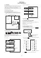
TABLE OF CONTENTS 4. TEST MODE 1. GENERAL Looking at the controls ...................................................... 4 4-1. 4-2. 4-3. 4-4. 4-5. 4-6. 2. SELF-DIAGNOSTIC 2-1. 2-2. 2-3. 2-4. 2-5. 2-6. General ............................................................................... Test Mode Setting .............................................................. Operation in Test Mode Setting ......................................... Releasing the Test Mode ........................................
SECTION 1 GENERAL –4– This section is extracted from instruction manual.
SECTION 2 SELF-DIAGNOSTIC 2-1. GENERAL 2) Remote controller LCD This set uses the self-diagnostic system in which if an error occurs in playback/recording mode, the error is detected by the model control and power control blocks of the microprocessor and information on the cause is stored as history in EEPROM. By viewing this history in test mode, it helps you to analyze a fault and determine its location. 888 ı All ON 2-2.
• Description of History Codes History code number 1st 0 1st 1 1st 2 N 0 N 1 N 2 N-1 0 N-1 1 N-1 2 N-2 0 N-2 1 N-2 2 R Description The first error 00 indicated The last error 00 indicated *1) Total recording time Total recording time is recorded in minutes as an index for load to the OP. It is recorded in hexadecimal format and up to 65,535 min. (about 886 discs of 74-minute disc) can be counted. It returns to “0000h” when recorder goes beyond this limit. Example : REC 000A n Approx. 10 min.
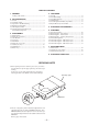
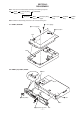
SECTION 3 DISASSEMBLY Note : This set can be disassemble according to the following sequence. Set Panel, Bottom Panel (SV) Assy, Front Connector LCD Module Main Board Panel (SV) Assy, Upper Cabinet (SV) Assy OP Block Assy Note : Follow the disassembly procedure in the numerical order given. 1 1.7x4.5, tapping 3-1. PANEL, BOTTOM 2 1.7x4.5, tapping 3 panel, bottom knob switch 3-2.
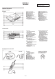
3-3. LCD MODULE 2 3 4 1 CN801 5 LCD module 3-4.
3-5. MAIN BOARD 1 1.7x4.5, tapping 2 1.7x4.5, tapping 4 MAIN board 3 claws 3-6. PANEL (SV) ASSY, UPPER 1 M1.
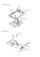
3-7. CABINET (SV) ASSY 1 MD, step 4 cabinet (SV) assy 2 MD, step 3 mechanism block assy 3-8. OP BLOCK ASSY 1 M1.4x3.0 locking 2 M1.4x3.
• Notes for Installation of the OP Block Assy • Be careful to avoid contact of the lens with the chassis when installing the OP block assy. • Location of the Flexible Board marked line Align this portion of the flexible board with the marked line on the holder. 3-9.
SECTION 4 TEST MODE 4-1. GENERAL This set provides the Overall adjustment mode (Assy mode) that allows CD and MO disk to be automatically adjusted when in the test mode. In this Assy mode, the system discriminates between CD and MO disk and then automatically perform adjustments for them in sequence. If a fault is found, the system displays its location. Also, the Servo mode allows each individual adjustment to be automatically adjusted. 4-2. TEST MODE SETTING See page 5. 4-3.
2. To perform automatic adjustment for an adjustment item with the mode number 030 to 047, press P key. If the result of adjustment is OK, the adjustment value changes from flashing to steady on and it is automatically written to EEPROM. (2) Audio Mode • How to Transfer in the Audio Mode Mode No.
Unit LCD display XX XX AUDIO Adjustment value (The data can be changed/written when flashing.) Mode No. (Lower two digits are displayed.) 3. Press the keys below to change the mode number. ( : Increases the one place. p : Sets the one place to 0. This key brings the ten place to 0 if the one place is 0. (3) Mechanism Mode • How to Transfer the Mode in the Mechanism Mode: Mode No.
(4) Power Mode Mode No. Test Description Indication value Remark 300 POWER test 310 POWER SUPPLY 311 DC IN +B voltage value 320 CHG TEST 321 Charging start 322 BATT under CHGMNT voltage value 323 BATT under +B CHGMNT voltage value 4-5. OVERALL ADJUSTMENT MODE (ASSY MODE) 1. Go into the test mode. 2. Press + key or VOLUME + and VOLUME + and VOLUME + and VOLUME + in this turn to set the power mode. 3. Insert the test CD (TDYS-1) or an available SONY CD. 4. Press ( key.
* For the mode numbers of 039 and 057, if the focus bias value is NG, the following display is repeated: 10. If the result of automatic adjustment is OK, the following display appears: 55 30 00 Focus bias value 11. If the result of automatic adjustment is NG, the following display appears: Mode No. While P key is being depressed 82 00 77 01 Result of adjustment NG Mode No. (lower two digits) Error code (01 to 04) Meaning of focus bias 12. If NG, set the servo mode.
Ver 1.4 2001. 01 SECTION 5 ELECTRICAL ADJUSTMENTS PRECAUTIONS FOR ADJUSTMENT MO TRAVERSE ADJUSTMENT 1) Perform all adjustments in the order given in the test mode. After adjusting, exit the test mode. 2) Use the following tools and measuring instruments. • Test CD TDYS-1 (Part No. : 4-963-646-01) • SONY MO disc available on the market • Laser power meter LPM-8001 (Part No. : J-2501-046-A) • Oscilloscope (Frequency band above 40 MHz. Perform the calibration of probe first before measuring.
LOW REFLECTION CD TRAVERSE ADJUSTMENT CD TRAVERSE ADJUSTMENT Connection : Connection : oscilloscope oscilloscope MAIN board MAIN board SP526 (TE) AP503 (VC) SP526 (TE) AP503 (VC) Adjustment Method : 1. Set the servo mode of the test mode (Mode : 000). 2. Press the ( key, and set the low reflection CD test adjustment mode (Mode : 040) using the VOLUME + or – key. 3. Insert any MO disk available on the market. 4.
CD RF LEVEL CHECK Adjustment Location : Connection : oscilloscope MAIN BOARD (SIDE B) MAIN board AP538 (RF) AP503 (VC) digital voltmeter MAIN board AP5117 (VCC) AP574 (LDIO) IC701 AP538 (RF) AP574 (LDIO) IC501 AP503 (VC) CN501 Adjustment Method : 1. Set the servo mode of the test mode (Mode : 000). 2. Press the ( key, and set the CD test adjustment mode (Mode : 050) using the VOLUME + or – key. 3. Press the = or + key and move the optical pick-up to the center circumference. 4.
SECTION 6 DIAGRAMS 6-1. IC PIN DESCRIPTIONS • IC601 CXD2652AR (DIGITAL SERVO, ENC/DEC & ATRAC MEMORY CONTROLLER) Pin No. 1 Pin name MNT 0 I/O O Pin Description Traverse count signal output. 2 MNT 1 O Track jump detect output. 3 MNT 2 — Not used (Open). 4 MNT 3 O Focus OK signal output. 5 SWDT I Inputs write data signal from system control (IC801). 6 SCLK I Inputs serial clock signal from system control (IC801). 7 XLAT I Inputs serial latch signal from system control (IC801).
Pin No. 56 Pin name AVSS I/O — Ground terminal. Pin Description 57 PDO — Not used (Open). 58 PCO O Decoder PLL master clock PLL phase comparison output. 59 FILI I Decoder PLL master clock PLL filter input. 60 FILO O Decoder PLL master clock PLL filter output. 61 CLTV I Decoder PLL master clock PLL VCO control voltage input. 62 PEAK I Inputs peak hold signal for light amount signal from RF amplifier (IC501).
• IC801 CXP740010 (SYSTEM CONTROL) Pin No. 1 Pin name CLKCS I/O O Pin Description Not used (Chip select output to real time clock). 2 XRST O Reset output. L : Reset 3 WRPWR O Laser power switching signal output. 4 TX O Write data transfer timing output. 5 SDI2 I Serial data input. 6 SDO2 O Serial data output. 7 SCK2 O Serial clock output. 8 RFSW O Power control output. 9 SSB I/O 10 SSB SCK I/O SSB clock signal input and output. (Not used (Open).
Pin No. 50 51 Pin name AVSS I/O — Pin Description Ground terminal for A/D converter. AVREF I A/D converter reference voltage input. 52 AVDD — 53 VLG2-MNT I 54 TEMP I Temp meter (IC802) input. 55 KEY3 I Key input. 56 KEY2 I Key input. 57 KEY1 I Key input. 58 XINT REC SW I Recording head position detect input. 59 UNREG MNT I 2.8 V voltage monitor input. 60 BAT VC I Battery detect signal input. 61 FG IN I FG input from motor driver (IC503).
MZ-R37 6-2. BLOCK DIAGRAM — SERVO SECTION — REC DRIVE IC901 (1/2) DIGITAL SERVO ENC/DEC & ATRAC MEMORY CONTROLER IC601 MODE1 8 MODE2 9 OVER WRITE HEAD DRIVE Q741,742 OVER WRITE HEAD HA EFM EFM 64 HB LOGIC 62 63 100 1 2 I J VC RF AUX SW 3 VC AUX PEAK BOTM PEAK/ BOTTOM ABCD AMP 4 5 6 7 A B C D RF AGC/ EQ RF AMP VC ABCD FOCUS ERROR AMP I-V CONV.
MZ-R37 6-3. BLOCK DIAGRAM — AUDIO SECTION — 6-4. BLOCK DIAGRAM — SYSTEM CONTROL SECTION — 2.8V AUDIO SECTION (Page 27) OPT CONTROL Q302 DIN ADC A SDTO LRCK BCK SDTI 4 2 3 5 SYSTEM CONTROL IC801 (3/3) WP AUDIO I/F CONTROL 44 7 RCH MIC AMP IC302 5 VCC (+2.8V) 8 25 1 46 26 MIC 2.5V R-CH CDTI CDTO CCLK KCS PD 29 REG IC304 15 14 13 12 47 MIC2.
MZ-R37 6-5. PRINTED WIRING BOARD • Semiconductor Location Ref. No.
MZ-R37 • Waveforms 6-6. SCHEMATIC DIAGRAM — MAIN SECTION (1/3) — • Refer to page 44 for IC Block Diagrams. 1 VOLT/DIV : 0.5V AC TIME/DIV : 1µsec 1.0±0.3Vp-p IC501 2 #• VOLT/DIV : 0.1V AC TIME/DIV : 0.1msec Approx. 0.5Vp-p IC501 3 @ª VOLT/DIV : 1V AC TIME/DIV : 5msec 2.8Vp-p 13.4msec IC601 4 !¡ VOLT/DIV : 1V AC TIME/DIV : 20nsec 2.6Vp-p 22.5MHz IC601 !¶ (Page 42) (Page 38) (Page 38) (Page 43) (Page 42) Note: • All capacitors are in µF unless otherwise noted.
MZ-R37 6-7. SCHEMATIC DIAGRAM — MAIN SECTION (2/3) — • Refer to page 44 for IC Block Diagrams. • Waveform 5 VOLT/DIV : 1V AC TIME/DIV : 20nsec (Page 43) 2.2Vp-p 12kHz IC801 $º (Page 42) (Page 37) (Page 37) (Page 37) (Page 37) Note: • All capacitors are in µF unless otherwise noted. pF: µµF 50 WV or less are not indicated except for electrolytics and tantalums. • All resistors are in Ω and 1/4 W or less unless otherwise specified. • % : indicates tolerance. ¢ • : internal component.
MZ-R37 6-8. SCHEMATIC DIAGRAM — MAIN SECTION (3/3) — • Refer to page 44 for IC Block Diagrams. (Page 37) (Page 37) (Page 38) (Page 38) Note: • All capacitors are in µF unless otherwise noted. pF: µµF 50 WV or less are not indicated except for electrolytics and tantalums. • All resistors are in Ω and 1/4 W or less unless otherwise specified. • % : indicates tolerance. • C : panel designation. • A : B+ Line. – 41 – – 42 – (Page 38) (Page 37) • Power voltage is dc 4.
IC501 CXA2523AR OPN OPO ADDC COMPP COMPO AGCI RF AGC RF PEAK 45 44 43 42 41 40 39 38 37 ADO HPF DPGA DBB DAC 35 34 33 32 RF AGC + – DQ0 1 DQ1 2 WE 3 EQ EQ ADCL VCMC VCMR ADCR 1 J 2 –1 – –2 – RFA3 HLPT –1 31 IPGAR 30 VRAD VC 29 LOUT2 A 3 P-P CBR REFRESH COUNTER –2 OFST CVB AUX SW PEAK3T 3T 3T PTGR WBL –2 ROW DECODERS BOTTOM PBSW GRVA 36 BOTM PBH –1 GRV + – 4 WBL 35 ABCD IVR 34 FE – – – – AA CONTROL REGISTER I/F A9 A0 A1 A2 A3 5 6 7 8 9 WORD
IC761 BA6966FV-E2 VOUT 20 WOUT 19 N.
VLG20 VLG20 L2L L2L PGND2 PGND2 L2H L2H VB VB VLI VLI 52 L4 RS 53 VG2 VLIM 54 CHGSW INM4 IC901 MPC18A35FTA 51 50 49 48 47 46 45 44 43 42 41 40 39 38 37 DCIN VR2 GENERATOR 36 PSL1 POWER SW PRE-DRIVER RF4 55 35 PSAM DGND 56 34 VAM3 33 VB 32 VB DCIN DC IN 57 VG1 58 C1H 59 C1L 60 VLG2 PRE-DRIVER CHARGE PUMP VLG1 PRE-DRIVER VDD 61 HB 62 HA 63 31 L1 30 L1 29 L1 DRIVE CONTROL 28 PGND 27 PGND 26 REMGND EFM EFM 64 L3 65 PGND3 66 VC 67 25 REMKEY 24 KEYON SETUP DC/DC OSC 23 INMU
SECTION 7 EXPLODED VIEWS NOTE: • The mechanical parts with no reference number in the exploded views are not supplied. • Items marked “*” are not stocked since they are seldom required for routine service. Some delay should be anticipated when ordering these items. • Abbreviation CND : Canadian model FR : French model • -XX and -X mean standardized parts, so they may have some difference from the original one. • Color Indication of Appearance Parts Example : KNOB, BALANCE (WHITE) ...
7-2. CABINET (SV) ASSY SECTION MT-MZR37-161 52 62 53 62 51 64 54 55 63 LCD1 65 56 69 57 67 58 66 59 69 60 65 60 70 71 Ref. No. Part No. Description Remark 51 51 52 53 54 X-4951-496-1 X-4951-497-1 4-963-883-41 X-4950-927-1 4-216-593-01 CABINET (S) ASSY (SILVER) CABINET (L) ASSY (BLUE) (EXCEPT US,CND) SCREW (M1.
7-3. MECHANISM DECK SECTION (MT-MZR37-161) 101 104 107 106 105 103 M1 119 108 110 110 108 120 117 111 118 112 115 122 114 M2 109 124 113 107 107 123 107 116 121 107 102 M3 The components identified by mark ! or dotted line with mark. ! are critical for safety. Replace only with part number specified. Ref. No. Part No. Description 101 102 103 104 105 X-4950-391-1 3-704-197-31 4-212-312-01 X-4950-390-1 4-995-585-11 HOLDER ASSY SCREW (M1.4X3.
SECTION 8 ELECTRICAL PARTS LIST MAIN NOTE: • Due to standardization, replacements in the parts list may be different from the parts specified in the diagrams or the components used on the set. • -XX and -X mean standardized parts, so they may have some difference from the original one. • RESISTORS All resistors are in ohms. METAL:Metal-film resistor. METAL OXIDE: Metal oxide-film resistor.
MAIN Ref. No. Part No. Description Part No. Description C511 C512 C513 C514 C515 1-115-467-11 1-162-968-11 1-162-970-11 1-162-965-11 1-125-837-11 CERAMIC CHIP CERAMIC CHIP CERAMIC CHIP CERAMIC CHIP CERAMIC CHIP 0.22uF 0.0047uF 0.01uF 0.0015uF 1uF 10% 10% 10% 10% 10% Remark 10V 50V 25V 50V 6.3V Ref. No. C825 C851 C852 C901 C902 1-162-969-11 1-162-970-11 1-107-826-11 1-135-259-11 1-135-259-11 CERAMIC CHIP CERAMIC CHIP CERAMIC CHIP TANTAL. CHIP TANTAL. CHIP 0.0068uF 0.01uF 0.
MAIN Ref. No. Part No. Description Part No.
MAIN Ref. No. Part No. Description Remark R202 1-218-875-11 RES,CHIP 15K R203 R205 R206 R207 1-218-855-11 1-218-863-11 1-218-871-11 1-218-871-11 2.2K 4.7K 10K 10K R208 R209 1-218-446-11 METAL CHIP 1-218-871-11 RES,CHIP 1 10K R209 1-218-875-11 RES,CHIP 15K R211 R212 1-218-891-11 RES,CHIP 1-218-887-11 RES,CHIP 68K 47K 5% 1/16W 0.50% 1/16W (EXCEPT FR) 0.50% 1/16W (FR) 0.50% 1/16W 0.
MZ-R37 MAIN Ref. No. Part No. Description R816 R818 R819 R820 R821 1-216-864-11 1-216-851-11 1-216-851-11 1-216-857-11 1-216-851-11 METAL CHIP METAL CHIP METAL CHIP METAL CHIP METAL CHIP 0 330K 330K 1M 330K 5% 5% 5% 5% 5% 1/16W 1/16W 1/16W 1/16W 1/16W Remark R822 R823 R824 R825 R826 1-218-887-11 1-216-857-11 1-216-833-11 1-218-911-11 1-216-864-11 RES,CHIP METAL CHIP METAL CHIP RES,CHIP METAL CHIP 47K 1M 10K 470K 0 0.50% 5% 5% 0.
MZ-R37 SERVICE MANUAL Ver 1.2 1999. 06 SUPPLEMENT-1 US Model Canadian Model AEP Model UK Model E Model Australian Model Tourist Model File this supplement with the service manual. Subject : Korean model Addition Korean model is added to the MZ-R37. This supplement-1 describes only differences from the MZ-R37 (E) model. Refer to the service manual for MZ-R37 (9-926-952-∏) for other information. • ACCESSORIES & PACKING MATERIALS Page 56 MZ-R37 (E model) MZ-R37 (Korean model) Ref. No. Part No.
MZ-R37 US Model Canadian Model AEP Model UK Model E Model Australian Model Tourist Model SERVICE MANUAL Ver 1.3 1999. 11 TABLE OF CONTENTS 1. PRINTED WIRING BOARD – EXCEPT US MODEL – ............................................. 3 2. PRINTED WIRING BOARD – US MODEL – ................................................................ 7 3. SCHEMATIC DIAGRAM – MAIN SECTION (1/3) – .......................................... 12 4. SCHEMATIC DIAGRAM – MAIN SECTION (2/3) – .........................................
MZ-R37 1.
MZ-R37 11 C929 R912 C927 C216 RB301 C312 R217 C214 C114 R117 R111 C112 R211 C103 C102 C202 C810 D801 10 12 R407 D408 R221 C219 R408 R107 C101 R106 IC303 C119 R120 R207 R206 R220 C201 15 13 R121 R209 R205 C206 E R203 R109 5 J302 LINE OUT C415 R406 C122 C222 C205 R409 C110 C210 C203 24 25 C105 R420 20 1 10 F C404 C405 R901 S881 DISPLAY R816 C221 C615 C121 11 G S805 Digital MEGA BASS J304 PHONES/REMOTE R832 R833 R881 4 AP401 3 D404 2 Q901 FB405
MZ-R37 2.
MZ-R37 11 C929 R912 C927 1 72 1 C426 C216 RB301 C312 R217 C214 C114 R117 R111 C112 R211 C103 C102 C202 12 13 R901 R816 5 C415 R406 C122 C222 10 12 R407 D408 R221 F C404 C405 G S805 Digital MEGA BASS J304 PHONES/REMOTE R832 R833 R881 E C219 R408 C119 R120 R121 R209 R205 C206 C106 R106 C121 R461 S881 DISPLAY 15 13 IC303 1 D801 R109 20 J302 LINE OUT R203 R107 C101 FB461 C615 C205 R420 R207 R206 R220 C201 15 C810 24 25 C105 R409 C110 C210 C203
MZ-R37 3. SCHEMATIC DIAGRAM — MAIN SECTION (1/3) — • Refer to page 15 for Waveforms. • Difference of Schematic Diagram (US Model) (Page 19) (Page 15) (Page 15) (Page 19) (Page 15) (Page 15) (Page 15) – 12 – – 13 – – 14 – Note: • All capacitors are in µF unless otherwise noted. pF: µµF 50 WV or less are not indicated except for electrolytics and tantalums. • All resistors are in Ω and 1/4 W or less unless otherwise specified. • % : indicates tolerance.
MZ-R37 4. SCHEMATIC DIAGRAM — MAIN SECTION (2/3) — • Waveforms 1 VOLT/DIV : 0.5V AC TIME/DIV : 1µsec (Page 20) 1.0±0.3Vp-p (Page 19) (Page 14) (Page 14) (Page 14) IC501 2 ek VOLT/DIV : 0.1V AC TIME/DIV : 0.1msec Approx. 0.5Vp-p IC501 3 wl VOLT/DIV : 1V AC TIME/DIV : 5msec (Page 14) 2.8Vp-p 13.4msec IC601 4 qa VOLT/DIV : 1V AC TIME/DIV : 20nsec 2.6Vp-p 22.5MHz IC601 5 qj VOLT/DIV : 1V AC TIME/DIV : 20nsec 2.
MZ-R37 5. SCHEMATIC DIAGRAM — MAIN SECTION (3/3) — (Page 14) (Page 14) (Page 15) (Page 15) Note: • All capacitors are in µF unless otherwise noted. pF: µµF 50 WV or less are not indicated except for electrolytics and tantalums. • All resistors are in Ω and 1/4 W or less unless otherwise specified. • % : indicates tolerance. • C : panel designation. • A : B+ Line. – 18 – – 19 – (Page 15) (Page 15) • Power voltage is dc 4.5 V and fed with regulated dc power supply from external power voltage jack.
MAIN 6. ELECTRICAL PARTS LIST NOTE: • Due to standardization, replacements in the parts list may be different from the parts specified in the diagrams or the components used on the set. • -XX and -X mean standardized parts, so they may have some difference from the original one. • RESISTORS All resistors are in ohms. METAL:Metal-film resistor. METAL OXIDE: Metal oxide-film resistor.
MAIN Ref. No. Part No. Description Part No. Description C504 C505 C506 C507 C508 1-162-966-11 1-162-970-11 1-107-826-11 1-162-969-11 1-107-826-11 CERAMIC CHIP CERAMIC CHIP CERAMIC CHIP CERAMIC CHIP CERAMIC CHIP 0.0022uF 0.01uF 0.1uF 0.0068uF 0.1uF 10% 10% 10% 10% 10% Remark 50V 25V 16V 25V 16V Ref. No. C807 C808 C810 C811 C812 1-162-927-11 1-164-156-11 1-162-970-11 1-162-970-11 1-125-837-11 CERAMIC CHIP CERAMIC CHIP CERAMIC CHIP CERAMIC CHIP CERAMIC CHIP 100PF 0.1uF 0.01uF 0.
MAIN Ref. No. Part No.
MAIN Ref. No. Part No. Description Part No. Description R112 R113 R115 R116 R117 1-218-887-11 1-216-864-11 1-218-847-11 1-218-831-11 1-218-883-11 METAL CHIP METAL CHIP METAL CHIP METAL CHIP METAL CHIP 47K 0 1K 220 33K 0.5% 5% 0.5% 0.5% 0.
MAIN Ref. No. Part No. Description Part No. Description R767 R768 R801 R803 R804 1-218-871-11 1-216-829-11 1-216-857-11 1-216-857-11 1-216-857-11 METAL CHIP METAL CHIP METAL CHIP METAL CHIP METAL CHIP 10K 4.7K 1M 1M 1M 0.5% 5% 5% 5% 5% 1/16W 1/16W 1/16W 1/16W 1/16W Remark Ref. No. R957 R959 R960 R961 R962 1-218-915-11 1-218-903-11 1-218-903-11 1-218-911-11 1-218-911-11 METAL CHIP METAL CHIP METAL CHIP METAL CHIP METAL CHIP 680K 220K 220K 470K 470K 0.5% 0.5% 0.5% 0.5% 0.
MZ-R37 7. Corrections • EXPLODED VIEWS 7-3. MECHANISM DECK SECTION Page 51 INCORRECT CORRECT Ref. No. Part No. Description Remark 0 122 A-3328-294-A OP SERVICE ASSY Part No. Description Remark X-4951-517-1 HEAD ASSY, OP • ELECTRICAL PARTS LIST/MISCELLANEOUS Page 56 INCORRECT CORRECT Ref. No. Part No. Description Remark X801 0 122 1-760-174-11 VIBRATOR, CERAMIC (12MHz) A-3328-294-A OP SERVICE ASSY Part No.