SERVICE MANUAL MODEL COMMANDER DEST. CHASSIS NO. KV-2199XDK RM-952 ME BG-3S CHASSIS MODEL COMMANDER DEST. CHASSIS NO.
KV-2199XDK RM-952 SPECIFICATIONS Note Power requirements 110-240 V AC, 50/60 Hz Power consumption (W) Indicated on the rear of the TV Television system B/G, D/K Color system PAL, PAL 60, SECAM, NTSC4.43, NTSC3.
KV-2199XDK RM-952 TABLE OF CONTENTS Section Title Page SELF DIAGNOSIS FUNCTION ................................ 4 Section 5-1. Block Diagram ......................................................... 5-2. Frame Schematic Diagram ...................................... 5-3 Circuit Boards Location .......................................... 5-4. Schematic Diagrams and Printed Wiring Boards ... (1) Schematic Diagram of A (1/2) Board ...................... (2) Schematic Diagram of A (2/2) Board .............
KV-2199XDK RM-952 SELF DIAGNOSTIC FUNCTION The units in this manual contain a self-diagnostic function. If an error occurs, the STANDBY/TIMER lamp will automatically begin to flash. The number of times the lamp flashes translates to a probable source of the problem. A definition of the STANDBY/TIMER lamp flash indicators is listed in the instruction manual for the user’s knowledge and reference.
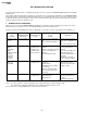
KV-2199XDK RM-952 2. DISPLAY OF STANDBY/TIMER LIGHT FLASH COUNT 2 times 5 times Lamp ON 0.3 sec. Lamp OFF 0.3 sec. Lamp OFF 3 sec. STANDBY/SLEEP lamp Diagnostic Item +B overcurrent/overvoltage Vertical deflection stopped Flash Count* 2 times White balance failure 5 times * One flash count is not used for self-diagnostic. 3. STOPPING THE STANDBY/TIMER FLASH Turn off the power switch on the TV main unit or unplug the power cord from the outlet to stop the STANDBY/TIMER lamp from flashing.
KV-2199XDK RM-952 4.
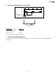
KV-2199XDK RM-952 6. SELF-DIAGNOSTIC CIRCUIT IC301 Y/CHROMA JUNGLE FROM CRT FROM [+B] Q604 C IC001 SYSTEM 21 IK-IN 18 MP/ PROTECT SDA 35 IO-8DAT 45 IC003 MEMORY 5 B-DAT O-LED 51 46 IO-SDAT [V] Q509/507 [+B overcurrent ªOCPº] Occurs when an overcurrent on the +B(135) line is detected by Q604. If Q604 go to ON and the voltage to pin 18 of IC301 should go down when V.SYNC is more than seven verticals in a period, the unit will automatically turn off.
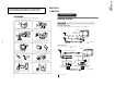
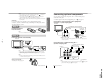
RM-952 SECTION 1 GENERAL Using Your New TV WARNING • Dangerously high voltages are present inside the TV. Getting Started • Operate the TV only between 110 – 240 V AC. Step 1 Connect the antenna If you wish to connect a VCR, see the “Connecting a VCR” diagram below. Do not open the cabinet and the rear cover of the TV. Refer servicing to qualified personnel. Install the TV in a stable position. Do not allow children to climb onto it.
Notes • If you connect a stereo VCR, connect the yellow plug to (the yellow jack) and the white plug to (the black jack). • If you connect a VCR to the ˘ (antenna) terminal, preset the signal output from the VCR to the program number 0 on the TV. • When no signal is input to the connected video equipment, the TV screen becomes blue. Connecting optional components You can connect optional video components, such as a VCR, multi disc player, camcorder or video game.
RM-952 To prevent the TV from falling, secure the TV using one of the following methods: You can preset up to 100 TV channels in numerical sequence from program number 1 using the remote and the buttons on your TV as well. Using Your New TV A With the supplied screws, attach the band to the TV stand and to the rear of the TV using the provided hole. or the cord or chain through the clamps to secure the TV against a wall or B Put pillar.
Presetting channels (continued) Presetting channels manually 1 To change the color system setting SELECT If the color is abnormal when receiving programs through the ˘ (antenna) terminal or the … (video input) jack MANUAL PROGRAM Using Your New TV 2 Press SELECT until “MANUAL PROGRAM” appears. Press + or –. VHF LOW B/G 3 4 – 11 – 5 Press PROGR +/– or the number buttons until the desired program number appears. or Press + or – until the desired channel picture appears. Press SELECT.
RM-952 Watching the TV (continued) ¤ u … ; This section explains functions used while watching the TV. Most operations can be done using the remote. 4 2 5 3 6 7 8 9 ÷ 0 JUMP SOUND MODE Á PROGR Using Your New TV 1 Additional tasks Number buttons JUMP . +/– PROGR +/– FAVORITE To Do this Turn off temporarily Press u. The u indicator on the TV lights up red. Turn off completely Press U on the TV. Mute the sound Press ¤. Watch the video input (VCR, camcorder, etc.
Advanced Operations Customizing the picture and sound Setting the Wake Up timer 1 Press until the desired period of time appears. SOUND MODE WAKE UP TIMER:12H00M After 12 hours Press u or set the Sleep timer if you want the TV to turn off automatically. SELECT + or – You can customize the picture and sound by selecting the picture and sound modes or by adjusting its settings.
RM-952 1 Press SELECT until the desired setting appears. SELECT PICTURE Each time you press SELECT, the setting item will change as follows: 2 PICTURE COLOR TREBLE You can display six of your favorite channels for quick and easy selection. You can change the favorite channel setting as well. 60 BRIGHT HUE* BASS SHARP 2 3 4 5 6 7 8 9 ÷ 0 JUMP SOUND MODE Á PROGR Number buttons PROGR +/– + or – FAVORITE Press + or – to adjust the item.
Additional Information Self-diagnosis function Blocking the channels (CHILD LOCK) 1 2 3 4 5 6 7 8 9 ÷ 0 JUMP SOUND MODE Á PROGR You can prevent a child from watching certain programs by using the buttons on the remote control. Your TV is equipped with a self-diagnosis function. If there is a problem with your TV, the u indicator flashes red. The number of times the u indicator flashes indicates the possible causes.
RM-952 Troubleshooting (continued) Symptom Snowy picture Solutions – 16 – Distorted picture Possible cause • The volume level is too low. • Press ¤ to cancel the muting. • The sound is muted. Dotted lines or stripes • Do not use a hair dryer or other equipment near the TV. • Adjust the antenna direction for minimum interference. Contact a Sony dealer for advice. • There is local interference from cars, neon signs, hair dryers, power generators, etc.
Identifying parts and controls Symptom Solutions Possible cause Lines moving across the TV screen • Use the fine tuning (FINE) function. (page 10) • There is interference from external sources, e.g., heavy machineries, nearby broadcast station. The u indicator on your TV flashes red a number of times between 3-second intervals. • Contact your nearest Sony service center. (page 18) • Your TV may need service.
RM-952 9 1 0 2 !¡ 1 2 3 4 5 6 7 8 9 ÷ 0 JUMP SOUND MODE Á PROGR !™ !£ !¶ 3 4 1 2 3 4 5 6 7 8 9 ÷ 0 JUMP SOUND MODE Á PROGR !§ 5 6 !¢ – 18 – 7 !∞ FAVORITE FAVORITE 8 TV 1 u (power) button (11) 2 ; (TV) button (12) 3 Number buttons (11) 4 JUMP button (12) 5 PROGR +/– buttons (11) 6 SELECT button (9) 7 PIC MODE button (14) 8 +/– buttons (8) 9 (display) button (12) !º ¤ (muting) button (12) !¡ … (video) button (12) !™ .
SECTION 2 DISASSEMBLY 2-1. REAR COVER REMOVAL 2-3. F BRACKET REMOVAL 2 Rear cover 3 One screw (+BVTP 3 × 12) 2 F board 1 Three connectors Lever – 19 – 1 two screw (+BVTP 4 × 16) 1 ten screws (+BVTP 4 × 16) 2-2. CHASSIS ASSY REMOVAL 2-4. SERVICE POSITION (Note: Remove F Bracket first.
RM-952 For replacement of the Multi Button, cut the welded portions from them, exchange with the new parts, and fix them with screws (+BVTP 3 x 12). 2-6. TERMINAL BRACKET REMOVAL 2-5-1. REPLACEMENT OF MULTI BUTTON Terminal board bracket Multi button screw (+BVTP 3 x 12) – 20 – Two screws (+BVTP 3 × 12) A board For replacement of the Light Guide, remove it, and exchange with the new part to fix. 2-7. DEGAUSS COIL REMOVAL 2-5-2.
• REMOVAL OF ANODE-CAP 2-8. PICTURE TUBE REMOVAL NOTE : After removing the anode, short circuit the anode of the picture tube and the anode cap to the metal chassis, CRT shield or carbon paint on the CRT. 3 F board 4 C3 board • REMOVING PROCEDURES 7 Neck assy 5 Deflection yoke a 2 A board a 6 Four screws (Tapping screws) 1 Turn up one side of the rubber cap in the direction indicated by the arrow a.
KV-2199XDK SECTION 3 RM-952 SET-UP ADJUSTMENTS • The following adjustments should be made when a complete realignment is required or a new picture tube is installed. • These adjustments should be performed with rated power supply voltage unless otherwise noted. Perform the adjustments in the following order : 1. Beam Landing Controls and switches should be set as follows unless otherwise noted: PICTURE control ........................................................... normal BRIGHTNESS control ....
KV-2199XDK RM-952 3-2. CONVERGENCE Preparation : • Before starting this adjustment, adjust the focus, horizontal size and vertical size. • • Minimize the brightness setting. Provide dot pattern. 1 V. STAT a b (1) b a b Horizontal and Vertical Static Convergence Center dot B B G G R R 2 H. STAT VR R a G b B R G B R H. STAT VR G B B G R V.STAT Magnet 3 a b b a B R G RV 702 b G R B 4 BMC (Hexapole) Magnet.
KV-2199XDK RM-952 4 Y separation axis correction magnet adjustment. Red Blue 1. Receive the cross-hatch signal and adjust [PICTURE] to [MIN] and [BRIGHTNESS] to [STANDARD] . Neck assy Neck assy 2. Adjust the Y separation axis correction magnet on the neck assembly so that the horizontal lines at the top and bottom of the screen are straight. Red Blue VM1 board VM1 board Note 1. The Red and Blue magnets should be equally far from the horizontal center line. 2.
KV-2199XDK RM-952 (3) Screen-corner Convergence 3-4. G2 (SCREEN) AND WHITE BALANCE ADJUSTMENTS b 1. G2 (SCREEN) ADJUSTMENT 1) Set the PICTURE to normal. a 2) Put to VIDEO input mode without signals. 3) Connect R, G and B of the C3 board cathode to the oscillo- a-d : screen-corner misconvergence c scope. 4) Adjust BRIGHTNESS to obtain the cathode voltage to the value d below. 5) Adjust G2 (Screen) on FBT until picture shows the point before cut-off.
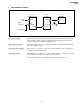
KV-2199XDK KV-2199XDK KV-2199XDK RM-952 RM-952 RM-952 SECTION 5 DIAGRAM 5-1. BLOCK DIAGRAM MAIN. TUVIF TU101 BTF-LG433(I) TV V in TV L in TV R in AUDIO PROSESSOR IC203 TDA7429S SP ASSY AUDIO OUT IC201 TA8223K CRT SOCKET 22 R out TV V in JACK BLOCK J401 4P V1 V in 43 12 V1 V in V1 L in YC JUNGLE IC301 CXA2130S 23 G out GREEN OUT G out 24 B out BLUE OUT B out DY Y21RSA-S C3 H. DRIVE H.
KV-2199XDK KV-2199XDK KV-2199XDK RM-952 RM-952 RM-952 5-3. CIRCUIT BOARDS LOCATION FBT 5-2.
KV-2199XDK RM-952 5-4. SCHEMATIC DIAGRAMS AND PRINTED WIRING BOARDS Note: • All capacitors are in µF unless otherwise noted. • All electrolytic capacitors are rated at 50V unless otherwise noted. • All resistors are in ohms. kΩ = 1000Ω, MΩ = 1000kΩ • Indication of resistance which does not have rating electrical power is as follows. Pitch: 5 mm Rating electrical power 1/4W (CHIP: 1/10W) • : nonflammable resistor. • ¢ : internal component. • : panel designation or adjustment for repair.
KV-2199XDK RM-952 A BOARD WAVEFORMS 1 2 3 4 PAL 4 SECAM 4.5Vp-p (V) 3.8Vp-p (V) 3.7Vp-p (V) 1.1Vp-p (H) 1.3Vp-p (H) 4 NTSC 3.58 4 NTSC 4.43 5 PAL/NTSC 3.58 5 SECAM/NTSC 4.43 6 1.2Vp-p (H) 0.8Vp-p (H) PAL : 0.9Vp-p (V) NTSC 3.58 : 0.6Vp-p (V) 1.0Vp-p (V) 0.8Vp-p (H) 7 PAL 7 SECAM 7 NTSC 3.58 7 NTSC 4.43 8 PAL 1.1Vp-p (H) 1.0Vp-p (H) 0.7Vp-p (H) 8 SECAM 8 NTSC 9 1.1Vp-p (H) 0.8Vp-p (H) 0.8Vp-p (H) 11 3.1Vp-p (H) 13 NTSC 4.43 0.9Vp-p (H) 12 PAL/NTSC 3.58 3.
(1) Schematic Diagram of A1/2 board 1 2 3 4 5 6 7 8 9 10 11 12 13 14 15 16 17 18 19 20 21 22 C336 0.1 25V B:CHIP 9V R349 10k :CHIP 9V Q312 D316 UDZS-TE17 PROTECT D315 1SS355TE PROTECT 2SA1162 :CHIP C333 # R348 10k :RN-CP D311 9V 1SS355TE R376 22k :CHIP C325 1 1 1SS355TE GND C OUT PROTECT D308 PROTECT 1SS355TE A GND GND 1 9V 5V 30V AS SDA :CHIP R112 SDA SCL L103 4.5 PS4 PS3 PS2 4.5 4.5 4.5 PS1 LP 4.5 4.5 LP1 HP1 HP2 4.5 4.5 8.9 VS 4.
(2) Schematic Diagram of A2/2 board 1 2 3 4 5 6 7 8 9 10 11 12 13 14 15 16 17 18 19 20 21 22 A CN507 # TO C3 BOARD C656 # 0.7 JW604 7.5MM RY601 DH5D1-0(M) 5 FB613 1.1UH 2 1 0 3 4 C611 0.0047 500V E C612 0.0047 500V E R625 # JW601 # R632 0.1 1/2W :RF FB601 1.1UH R646 3W :RS 15k C618 680p 1.5kV FB615 1.1UH C613 330 450V FB602 1.1UH C620 470p CH:CHIP R628 # JW603 10.0MM C610 10 0.2 -2.3 RY600 # 0 R640 680 R641 0.
KV-2199XDK KV-2199XDK KV-2199XDK RM-952 RM-952 RM-952 A BOARD IC TO 8-BIT TIMER 1 XLC EXLC R G B I YS YM HSYNC VSYNC HS0 PORT A 8-BIT TIMER/ COUNTER 0 8 PB0~PB7 6 PC0~PC5 2 PC6~PC7 2 8 PD0~PD7 2 PE0~PE1 2 PE2~PE3 3 PE4~PE6 8 PF0~PF7 5 PG3~PG6*, PG7 PORT D EC RAM 352/704/1536 BYTES PA0~PA7 PORT B SERIAL INTERFACE UNIT ROM 12K/16K/24K/32K 40K/48K/60K BYTES 8 PORT C FIFO CLOCK GENERATOR /SYSTEM CONTROL 2 PRESCALER/ TIME-BASE TIMER ON SCREEN DISPLAY PORT E S1 SO SC
(3) Schematic Diagrams of C3 and VM1 boards 1 2 3 4 5 6 7 8 9 10 C3 (RGB OUT) L701 G2 14 15 16 17 18 R5917 820 0.5W :RN Q5905 2SC2458TP-YGR BUFFER 19 20 21 22 C704 0.022 400V :PP C701 0.0047 2kV E G2 1 200V E 3 H1 R715 1k 1/2W 1 R713 1k 1/2W R734 100 1/2W CN705 # L710 R708 6.8 2W :RS 3 1 CN706 # L712 D C5901 # L5901 C737 470p B R723 270k :RN E 4.6 8.7 1.5 8.2 R722 1k :FPRD C709 470p B 4.7 C708 470p B R721 680k :RN 9V 1.7 1.9 R727 2.2k 150 R730 R 8.
KV-2199XDK KV-2199XDK RM-952 RM-952 (4) Schematic Diagram of F board 1 2 3 4 5 6 7 A B F [CISPR] PRINTED WIRING BOARD C – F Board – F (CISPR) D D E AC OUT 2 AC OUT 2 1 1 2 CN4602 2P :VH CN4603 1P :TAB TO A BOARD CN601 C654 0.0047 250V TO A BOARD CN104 1 3 2 R4601 1M 1/2W T4602 # 4 1 AC IN T4601 T.L.F 4 AC IN VDR461 ERZV14D621 3 F4601 T3.15A FUSE 250V CN4601 2P :VH C4602 0.47 250V :PP C4601 # GND B-SSS10217-ME.-F..
VM1 C3 [VELOCITY MODULATION] KV-2199XDK KV-2199XDK RM-952 RM-952 [RGB OUT] PRINTED WIRING BOARDS – C3 Board – – VM1 Board – C3 BOARD WAVEFORMS 1 2 PAL 2 SECAM 25Vp-p (H) 89Vp-p (H) 90Vp-p (H) 2 NTSC 3.58 2 NTSC 4.
KV-2199XDK KV-2199XDK RM-952 RM-952 5-5. SEMICONDUCTORS DIODE TRANSISTOR EG010CV0 4 CATHODE 3 1 LETTER SIDE C ANODE 4 2SC2611 UN2111 UN2211 UN2213 UN2216 2SA1162-G 2SC2712-YG 2SD2114K 1 3 B 1 E E 2 ANODE D4SB60L D1NS4 RD20ES-B2 RD30ESB2 RD39ES-B2 RD6.8ES-B1 RD9.
KV-2199XDK KV-2199XDK RM-952 RM-952 SECTION 6 EXPLODED VIEW NOTE: • Items with no part number and no description are not stocked because they are seldom required for routine service. • The construction parts of an assembled part are indicated with a collation number in the remark column. • Items marked " * " are not stocked since they are seldom required for routine ser vice. Some delay should be anticipated when ordering these items.
KV-2199XDK RM-952 The components identified by shading and mark ! are critical for safety. Replace only with part number specified. SECTION 7 ELECTRICAL PARTS LIST REF. NO. PART NO. NOTE: DESCRIPTION REMARK REF. NO. PART NO. The components identified by shading and mark ! are critical for safety. Replace only with part number specified. • Items marked " ∗ " are not stocked since they are seldom required for routine service. Some delay should be anticipated when ordering these items.
KV-2199XDK RM-952 The components identified by shading and mark ! are critical for safety. Replace only with part number specified. A REF. NO. PART NO. DESCRIPTION REMARK C243 C244 C245 1-216-295-91 1-164-700-11 1-164-346-11 SHORT CERAMIC CHIP CERAMIC CHIP 0 0.68MF 1MF C246 C248 C249 C251 C252 1-163-018-00 1-163-010-11 1-164-004-11 1-163-017-00 1-164-346-11 CERAMIC CHIP CERAMIC CHIP CERAMIC CHIP CERAMIC CHIP CERAMIC CHIP 0.0056MF 0.0012MF 0.1MF 0.
KV-2199XDK RM-952 The components identified by shading and mark ! are critical for safety. Replace only with part number specified. REF. NO. PART NO. A DESCRIPTION REMARK C614 C616 1-126-964-11 1-130-202-00 ELECT FILM 10MF 0.022MF 20% 10% 50V 400V C617 C618 C619 C620 C621 1-107-792-11 1-125-893-11 1-119-886-51 1-163-133-00 1-102-114-00 CERAMIC FILM CERAMIC CERAMIC CHIP CERAMIC 100PF 680PF 470PF 470PF 470PF 5% 3% 10% 5% 10% 1KV 1.
KV-2199XDK RM-952 The components identified by shading and mark ! are critical for safety. Replace only with part number specified. A REF. NO. PART NO. DESCRIPTION REMARK D611 D613 D614 8-719-075-73 8-719-046-74 8-719-046-74 DIODE 10ELS2N-TB5 DIODE AU-01Z-V1 DIODE AU-01Z-V1 D618 D620 D622 D623 D624 8-719-067-18 8-719-110-72 8-719-071-39 8-719-978-65 8-719-073-01 DIODE RN4Z DIODE RD30ESB2 DIODE FMU-G26S DIODE DTZ-TT11-15B DIODE MA111-(K8).
KV-2199XDK RM-952 The components identified by shading and mark ! are critical for safety. Replace only with part number specified. REF. NO. PART NO.
KV-2199XDK RM-952 The components identified by shading and mark ! are critical for safety. Replace only with part number specified. A REF. NO. PART NO. DESCRIPTION REMARK R112 R113 R202 R203 R204 1-216-025-91 1-216-047-91 1-216-053-00 1-216-063-91 1-216-061-00 RES,CHIP RES,CHIP RES,CHIP RES,CHIP RES,CHIP 100 820 1.5K 3.9K 3.
KV-2199XDK RM-952 The components identified by shading and mark ! are critical for safety. Replace only with part number specified. REF. NO. PART NO. A DESCRIPTION REMARK R537 R540 R541 R542 R543 1-208-814-91 1-216-065-91 1-216-065-91 1-216-295-91 1-249-426-11 RES,CHIP RES,CHIP RES,CHIP SHORT CARBON 22K 4.7K 4.7K 0 5.6K 0.
KV-2199XDK RM-952 The components identified by shading and mark ! are critical for safety. Replace only with part number specified. A C3 REF. NO. PART NO.
KV-2199XDK RM-952 The components identified by shading and mark ! are critical for safety. Replace only with part number specified. REF. NO. PART NO. C3 F VM1 DESCRIPTION REMARK R712 R713 R714 1-215-922-11 1-247-752-11 1-215-922-11 METAL OXIDE CARBON METAL OXIDE 6.8K 1K 6.
KV-2199XDK RM-952 The components identified by shading and mark ! are critical for safety. Replace only with part number specified. VM1 REF. NO. PART NO. DESCRIPTION REMARK L5901 L5902 1-414-187-11 1-414-856-11 INDUCTOR INDUCTOR REF. NO. PART NO.