
Manual

DDR SODIMM
Product Datasheet
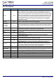
Pin Description
Symbol Type Description
A0–A12 Input
Address inputs: Provide the row address for ACTIVE commands, and the
column address and auto precharge bit (A10) for READ/WRITE commands, to
select one location out of the memory array in the respective device bank. A10
sampled during a PRECHARGE command determines whether the PRECHARGE
applies to one device bank (A10 LOW, device bank selected by BA0, BA1) or all
device banks (A10 HIGH). The address inputs also provide the op-code during a
MODE REGISTER SET command. BA0 and BA1 define which mode register
(mode register or extended mode register) is loaded during the LOAD MODE
REGISTER command.
BA0–BA1 Input
Bank address: BA0 and BA1 define the device bank to which an ACTIVE, READ,
WRITE, or PRECHARGE command is being applied.
CK0, CK0#,
CK1, CK1#,
CK2, CK2#
Input
Clock: CK and CK# are differential clock inputs. All address and control input
signals are sampled on the crossing of the positive edge of CK and the negative
edge of CK#. Output data (DQ and DQS) is referenced to the crossings of CK and
CK#.
CKE0 ,CKE1 Input
Clock enable: CKE (registered HIGH) activates and CKE (registered LOW)
deactivates the internal clock, input buffers, and output drivers.
RAS#, CAS#,
WE#
Input
Command inputs: RAS#, CAS#, and WE# (along with S#) define the command
being entered.
S0#, S1# Input
Chip select: S# enables (registered LOW) and disables (registered HIGH) the
command decoder.
SA0–SA2 Input
Presence-detect address inputs: These pins are used to configure the
presence-detect devices.
SCL Input
Serial clock for presence-detect: SCL is used to synchronize the
presence-detect data transfer to and from the module.
SDA I/O
Serial presence-detect data: SDA is a bidirectional pin used to transfer
addresses and data into and out of the presence-detect portion of the module.
DM0–DM7 I/O
Input data mask: DM is an input mask signal for write data. Input data is
masked when DM is sampled HIGH, along with that input data, during a write
access. DM is sampled on both edges of DQS. Although DM pins are input-only,
the DM loading is designed to match that of DQ and DQS pins.
DQ0–DQ63 I/O Data input/output: Bidirectional data bus.
DQS0–DQS7,
I/O
Data strobe: Output with read data, input with write data. DQS is edge aligned
with read data, center-aligned with write data. Used to capture data.
V
DD
/V
DDQ
Supply Power supply: 2.5V ±0.1V.
V
DDSPD
Supply Serial EEPROM positive power supply: +2.3V to +3.6V.
V
REF
Supply SSTL_2 reference voltage. (V
DD
/2)
V
SS
Supply Ground.
NC – No connect: These pins are not connected on the module.
Rev. 1.0 Oct. 2011
4