
Datasheet

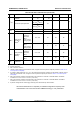
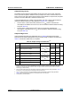
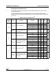
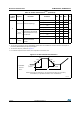
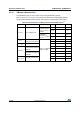
Table Of Contents
- Table 1. Device summary
- 1 Introduction
- 2 Description
- Table 2. STM32F405xx and STM32F407xx: features and peripheral counts (continued)
- 2.1 Full compatibility throughout the family
- 2.2 Device overview
- 2.2.1 ARM® Cortex®-M4 core with FPU and embedded Flash and SRAM
- 2.2.2 Adaptive real-time memory accelerator (ART Accelerator™)
- 2.2.3 Memory protection unit
- 2.2.4 Embedded Flash memory
- 2.2.5 CRC (cyclic redundancy check) calculation unit
- 2.2.6 Embedded SRAM
- 2.2.7 Multi-AHB bus matrix
- 2.2.8 DMA controller (DMA)
- 2.2.9 Flexible static memory controller (FSMC)
- 2.2.10 Nested vectored interrupt controller (NVIC)
- 2.2.11 External interrupt/event controller (EXTI)
- 2.2.12 Clocks and startup
- 2.2.13 Boot modes
- 2.2.14 Power supply schemes
- 2.2.15 Power supply supervisor
- 2.2.16 Voltage regulator
- 2.2.17 Regulator ON/OFF and internal reset ON/OFF availability
- 2.2.18 Real-time clock (RTC), backup SRAM and backup registers
- 2.2.19 Low-power modes
- 2.2.20 VBAT operation
- 2.2.21 Timers and watchdogs
- 2.2.22 Inter-integrated circuit interface (I²C)
- 2.2.23 Universal synchronous/asynchronous receiver transmitters (USART)
- 2.2.24 Serial peripheral interface (SPI)
- 2.2.25 Inter-integrated sound (I2S)
- 2.2.26 Audio PLL (PLLI2S)
- 2.2.27 Secure digital input/output interface (SDIO)
- 2.2.28 Ethernet MAC interface with dedicated DMA and IEEE 1588 support
- 2.2.29 Controller area network (bxCAN)
- 2.2.30 Universal serial bus on-the-go full-speed (OTG_FS)
- 2.2.31 Universal serial bus on-the-go high-speed (OTG_HS)
- 2.2.32 Digital camera interface (DCMI)
- 2.2.33 Random number generator (RNG)
- 2.2.34 General-purpose input/outputs (GPIOs)
- 2.2.35 Analog-to-digital converters (ADCs)
- 2.2.36 Temperature sensor
- 2.2.37 Digital-to-analog converter (DAC)
- 2.2.38 Serial wire JTAG debug port (SWJ-DP)
- 2.2.39 Embedded Trace Macrocell™
- 3 Pinouts and pin description
- 4 Memory mapping
- 5 Electrical characteristics
- 5.1 Parameter conditions
- 5.2 Absolute maximum ratings
- 5.3 Operating conditions
- 5.3.1 General operating conditions
- 5.3.2 VCAP_1/VCAP_2 external capacitor
- 5.3.3 Operating conditions at power-up / power-down (regulator ON)
- 5.3.4 Operating conditions at power-up / power-down (regulator OFF)
- 5.3.5 Embedded reset and power control block characteristics
- 5.3.6 Supply current characteristics
- Table 20. Typical and maximum current consumption in Run mode, code with data processing running from Flash memory (ART accelerator enabled) or RAM
- Table 21. Typical and maximum current consumption in Run mode, code with data processing running from Flash memory (ART accelerator disabled)
- Table 22. Typical and maximum current consumption in Sleep mode
- Table 23. Typical and maximum current consumptions in Stop mode
- Table 24. Typical and maximum current consumptions in Standby mode
- Table 25. Typical and maximum current consumptions in VBAT mode
- Table 26. Typical current consumption in Run mode, code with data processing running from Flash memory, regulator ON (ART accelerator enabled except prefetch), VDD = 1.8 V
- Table 27. Switching output I/O current consumption
- Table 28. Peripheral current consumption
- 5.3.7 Wakeup time from low-power mode
- 5.3.8 External clock source characteristics
- 5.3.9 Internal clock source characteristics
- 5.3.10 PLL characteristics
- 5.3.11 PLL spread spectrum clock generation (SSCG) characteristics
- 5.3.12 Memory characteristics
- 5.3.13 EMC characteristics
- 5.3.14 Absolute maximum ratings (electrical sensitivity)
- 5.3.15 I/O current injection characteristics
- 5.3.16 I/O port characteristics
- 5.3.17 NRST pin characteristics
- 5.3.18 TIM timer characteristics
- 5.3.19 Communications interfaces
- Table 54. I2C analog filter characteristics
- Table 55. SPI dynamic characteristics
- Table 56. I2S dynamic characteristics
- Table 57. USB OTG FS startup time
- Table 58. USB OTG FS DC electrical characteristics
- Table 59. USB OTG FS electrical characteristics
- Table 60. USB HS DC electrical characteristics
- Table 61. USB HS clock timing parameters
- Table 62. ULPI timing
- Table 63. Ethernet DC electrical characteristics
- Table 64. Dynamic characteristics: Eternity MAC signals for SMI
- Table 65. Dynamic characteristics: Ethernet MAC signals for RMII
- Table 66. Dynamic characteristics: Ethernet MAC signals for MII
- 5.3.20 CAN (controller area network) interface
- 5.3.21 12-bit ADC characteristics
- 5.3.22 Temperature sensor characteristics
- 5.3.23 VBAT monitoring characteristics
- 5.3.24 Embedded reference voltage
- 5.3.25 DAC electrical characteristics
- 5.3.26 FSMC characteristics
- Table 75. Asynchronous non-multiplexed SRAM/PSRAM/NOR read timings
- Table 76. Asynchronous non-multiplexed SRAM/PSRAM/NOR write timings
- Table 77. Asynchronous multiplexed PSRAM/NOR read timings
- Table 78. Asynchronous multiplexed PSRAM/NOR write timings
- Table 79. Synchronous multiplexed NOR/PSRAM read timings
- Table 80. Synchronous multiplexed PSRAM write timings
- Table 81. Synchronous non-multiplexed NOR/PSRAM read timings
- Table 82. Synchronous non-multiplexed PSRAM write timings
- Table 83. Switching characteristics for PC Card/CF read and write cycles in attribute/common space
- Table 84. Switching characteristics for PC Card/CF read and write cycles in I/O space
- Table 85. Switching characteristics for NAND Flash read cycles
- Table 86. Switching characteristics for NAND Flash write cycles
- 5.3.27 Camera interface (DCMI) timing specifications
- 5.3.28 SD/SDIO MMC card host interface (SDIO) characteristics
- 5.3.29 RTC characteristics
- 6 Package information
- 7 Part numbering
- Appendix A Application block diagrams
- 8 Revision history

DocID022152 Rev 8 113/202
STM32F405xx, STM32F407xx Electrical characteristics
Static latchup
Two complementary static tests are required on six parts to assess the latchup
performance:
• A supply overvoltage is applied to each power supply pin
• A current injection is applied to each input, output and configurable I/O pin
These tests are compliant with EIA/JESD 78A IC latchup standard.
5.3.15 I/O current injection characteristics
As a general rule, current injection to the I/O pins, due to external voltage below V
SS
or
above V
DD
(for standard, 3 V-capable I/O pins) should be avoided during normal product
operation. However, in order to give an indication of the robustness of the microcontroller in
cases when abnormal injection accidentally happens, susceptibility tests are performed on a
sample basis during device characterization.
Functional susceptibilty to I/O current injection
While a simple application is executed on the device, the device is stressed by injecting
current into the I/O pins programmed in floating input mode. While current is injected into
the I/O pin, one at a time, the device is checked for functional failures.
The failure is indicated by an out of range parameter: ADC error above a certain limit (>5
LSB TUE), out of conventional limits of induced leakage current on adjacent pins (out of
5
μA/+0 μA range), or other functional failure (for example reset, oscillator frequency
deviation).
Negative induced leakage current is caused by negative injection and positive induced
leakage current by positive injection.
The test results are given in Table 47.
Table 46. Electrical sensitivities
Symbol Parameter Conditions Class
LU Static latch-up class T
A
= +105 °C conforming to JESD78A II level A