
Datasheet
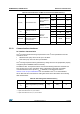

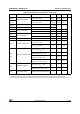
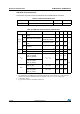
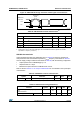
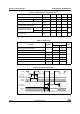
Table Of Contents
- Table 1. Device summary
- 1 Introduction
- 2 Description
- Table 2. STM32F405xx and STM32F407xx: features and peripheral counts (continued)
- 2.1 Full compatibility throughout the family
- 2.2 Device overview
- 2.2.1 ARM® Cortex®-M4 core with FPU and embedded Flash and SRAM
- 2.2.2 Adaptive real-time memory accelerator (ART Accelerator™)
- 2.2.3 Memory protection unit
- 2.2.4 Embedded Flash memory
- 2.2.5 CRC (cyclic redundancy check) calculation unit
- 2.2.6 Embedded SRAM
- 2.2.7 Multi-AHB bus matrix
- 2.2.8 DMA controller (DMA)
- 2.2.9 Flexible static memory controller (FSMC)
- 2.2.10 Nested vectored interrupt controller (NVIC)
- 2.2.11 External interrupt/event controller (EXTI)
- 2.2.12 Clocks and startup
- 2.2.13 Boot modes
- 2.2.14 Power supply schemes
- 2.2.15 Power supply supervisor
- 2.2.16 Voltage regulator
- 2.2.17 Regulator ON/OFF and internal reset ON/OFF availability
- 2.2.18 Real-time clock (RTC), backup SRAM and backup registers
- 2.2.19 Low-power modes
- 2.2.20 VBAT operation
- 2.2.21 Timers and watchdogs
- 2.2.22 Inter-integrated circuit interface (I²C)
- 2.2.23 Universal synchronous/asynchronous receiver transmitters (USART)
- 2.2.24 Serial peripheral interface (SPI)
- 2.2.25 Inter-integrated sound (I2S)
- 2.2.26 Audio PLL (PLLI2S)
- 2.2.27 Secure digital input/output interface (SDIO)
- 2.2.28 Ethernet MAC interface with dedicated DMA and IEEE 1588 support
- 2.2.29 Controller area network (bxCAN)
- 2.2.30 Universal serial bus on-the-go full-speed (OTG_FS)
- 2.2.31 Universal serial bus on-the-go high-speed (OTG_HS)
- 2.2.32 Digital camera interface (DCMI)
- 2.2.33 Random number generator (RNG)
- 2.2.34 General-purpose input/outputs (GPIOs)
- 2.2.35 Analog-to-digital converters (ADCs)
- 2.2.36 Temperature sensor
- 2.2.37 Digital-to-analog converter (DAC)
- 2.2.38 Serial wire JTAG debug port (SWJ-DP)
- 2.2.39 Embedded Trace Macrocell™
- 3 Pinouts and pin description
- 4 Memory mapping
- 5 Electrical characteristics
- 5.1 Parameter conditions
- 5.2 Absolute maximum ratings
- 5.3 Operating conditions
- 5.3.1 General operating conditions
- 5.3.2 VCAP_1/VCAP_2 external capacitor
- 5.3.3 Operating conditions at power-up / power-down (regulator ON)
- 5.3.4 Operating conditions at power-up / power-down (regulator OFF)
- 5.3.5 Embedded reset and power control block characteristics
- 5.3.6 Supply current characteristics
- Table 20. Typical and maximum current consumption in Run mode, code with data processing running from Flash memory (ART accelerator enabled) or RAM
- Table 21. Typical and maximum current consumption in Run mode, code with data processing running from Flash memory (ART accelerator disabled)
- Table 22. Typical and maximum current consumption in Sleep mode
- Table 23. Typical and maximum current consumptions in Stop mode
- Table 24. Typical and maximum current consumptions in Standby mode
- Table 25. Typical and maximum current consumptions in VBAT mode
- Table 26. Typical current consumption in Run mode, code with data processing running from Flash memory, regulator ON (ART accelerator enabled except prefetch), VDD = 1.8 V
- Table 27. Switching output I/O current consumption
- Table 28. Peripheral current consumption
- 5.3.7 Wakeup time from low-power mode
- 5.3.8 External clock source characteristics
- 5.3.9 Internal clock source characteristics
- 5.3.10 PLL characteristics
- 5.3.11 PLL spread spectrum clock generation (SSCG) characteristics
- 5.3.12 Memory characteristics
- 5.3.13 EMC characteristics
- 5.3.14 Absolute maximum ratings (electrical sensitivity)
- 5.3.15 I/O current injection characteristics
- 5.3.16 I/O port characteristics
- 5.3.17 NRST pin characteristics
- 5.3.18 TIM timer characteristics
- 5.3.19 Communications interfaces
- Table 54. I2C analog filter characteristics
- Table 55. SPI dynamic characteristics
- Table 56. I2S dynamic characteristics
- Table 57. USB OTG FS startup time
- Table 58. USB OTG FS DC electrical characteristics
- Table 59. USB OTG FS electrical characteristics
- Table 60. USB HS DC electrical characteristics
- Table 61. USB HS clock timing parameters
- Table 62. ULPI timing
- Table 63. Ethernet DC electrical characteristics
- Table 64. Dynamic characteristics: Eternity MAC signals for SMI
- Table 65. Dynamic characteristics: Ethernet MAC signals for RMII
- Table 66. Dynamic characteristics: Ethernet MAC signals for MII
- 5.3.20 CAN (controller area network) interface
- 5.3.21 12-bit ADC characteristics
- 5.3.22 Temperature sensor characteristics
- 5.3.23 VBAT monitoring characteristics
- 5.3.24 Embedded reference voltage
- 5.3.25 DAC electrical characteristics
- 5.3.26 FSMC characteristics
- Table 75. Asynchronous non-multiplexed SRAM/PSRAM/NOR read timings
- Table 76. Asynchronous non-multiplexed SRAM/PSRAM/NOR write timings
- Table 77. Asynchronous multiplexed PSRAM/NOR read timings
- Table 78. Asynchronous multiplexed PSRAM/NOR write timings
- Table 79. Synchronous multiplexed NOR/PSRAM read timings
- Table 80. Synchronous multiplexed PSRAM write timings
- Table 81. Synchronous non-multiplexed NOR/PSRAM read timings
- Table 82. Synchronous non-multiplexed PSRAM write timings
- Table 83. Switching characteristics for PC Card/CF read and write cycles in attribute/common space
- Table 84. Switching characteristics for PC Card/CF read and write cycles in I/O space
- Table 85. Switching characteristics for NAND Flash read cycles
- Table 86. Switching characteristics for NAND Flash write cycles
- 5.3.27 Camera interface (DCMI) timing specifications
- 5.3.28 SD/SDIO MMC card host interface (SDIO) characteristics
- 5.3.29 RTC characteristics
- 6 Package information
- 7 Part numbering
- Appendix A Application block diagrams
- 8 Revision history

Electrical characteristics STM32F405xx, STM32F407xx
128/202 DocID022152 Rev 8
USB OTG FS characteristics
This interface is present in both the USB OTG HS and USB OTG FS controllers.
Table 57. USB OTG FS startup time
Symbol Parameter Max Unit
t
STARTUP
(1)
1. Guaranteed by design.
USB OTG FS transceiver startup time 1 µs
Table 58. USB OTG FS DC electrical characteristics
Symbol Parameter Conditions Min.
(1)
1. All the voltages are measured from the local ground potential.
Typ. Max.
(1)
Unit
Input
levels
V
DD
USB OTG FS operating
voltage
-3.0
(2)
2. The STM32F405xx and STM32F407xx USB OTG FS functionality is ensured down to 2.7 V but not the full
USB OTG FS electrical characteristics which are degraded in the 2.7-to-3.0 V V
DD
voltage range.
-3.6V
V
DI
(3)
3. Guaranteed by design.
Differential input sensitivity
I(USB_FS_DP/DM,
USB_HS_DP/DM)
0.2 - -
VV
CM
(3)
Differential common mode
range
Includes V
DI
range 0.8 - 2.5
V
SE
(3)
Single ended receiver
threshold
- 1.3 - 2.0
Output
levels
V
OL
Static output level low R
L
of 1.5 kΩ to 3.6 V
(4)
4.
R
L
is the load connected on the USB OTG FS drivers
--0.3
V
V
OH
Static output level high R
L
of 15 kΩ to V
SS
(4)
2.8 - 3.6
R
PD
PA11, PA12, PB14, PB15
(USB_FS_DP/DM,
USB_HS_DP/DM)
V
IN
= V
DD
17 21 24
kΩ
PA9, PB13
(OTG_FS_VBUS,
OTG_HS_VBUS)
0.65 1.1 2.0
R
PU
PA12, PB15 (USB_FS_DP,
USB_HS_DP)
V
IN
= V
SS
1.5 1.8 2.1
PA9, PB13
(OTG_FS_VBUS,
OTG_HS_VBUS)
V
IN
= V
SS
0.25 0.37 0.55