
Data Sheet
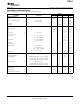
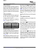

ELECTRICAL CHARACTERISTICS
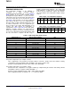
TMP102
www.ti.com
............................................................................................................................................... SBOS397B – AUGUST 2007 – REVISED OCTOBER 2008
At T
A
= +25 ° C and V
S
= +1.4V to +3.6V, unless otherwise noted.
TMP102
PARAMETER CONDITIONS MIN TYP MAX UNIT
TEMPERATURE INPUT
Range – 40 +125 ° C
Accuracy (Temperature Error) – 25 ° C to +85 ° C 0.5 2 ° C
– 40 ° C to +125 ° C 1 3 ° C
vs Supply 0.2 0.5 ° C/V
Resolution 0.0625 ° C
DIGITAL INPUT/OUTPUT
Input Logic Levels:
V
IH
0.7 (V+) 3.6 V
V
IL
– 0.5 0.3 (V+) V
Input Current I
IN
0 < V
IN
< 3.6V 1 µ A
Output Logic Levels:
V
OL
SDA V+ > 2V, I
OL
= 3mA 0 0.4 V
V+ < 2V, I
OL
= 3mA 0 0.2 (V+) V
V
OL
ALERT V+ > 2V, I
OL
= 3mA 0 0.4 V
V+ < 2V, I
OL
= 3mA 0 0.2 (V+) V
Resolution 12 Bit
Conversion Time 26 35 ms
Conversion Modes CR1 = 0, CR0 = 0 0.25 Conv/s
CR1 = 0, CR0 = 1 1 Conv/s
CR1 = 1, CR0 = 0 (default) 4 Conv/s
CR1 = 1, CR0 = 1 8 Conv/s
Timeout Time 30 40 ms
POWER SUPPLY
Operating Supply Range +1.4 +3.6 V
Quiescent Current I
Q
Serial Bus Inactive, CR1 = 1, CR0 = 0 (default) 7 10 µ A
Serial Bus Active, SCL Frequency = 400kHz 15 µ A
Serial Bus Active, SCL Frequency = 3.4MHz 85 µ A
Shutdown Current I
SD
Serial Bus Inactive 0.5 1 µ A
Serial Bus Active, SCL Frequency = 400kHz 10 µ A
Serial Bus Active, SCL Frequency = 3.4MHz 80 µ A
TEMPERATURE RANGE
Specified Range – 40 +125 ° C
Operating Range – 55 +150 ° C
Thermal Resistance, SOT563 θ
JA
260 ° C/W
Copyright © 2007 – 2008, Texas Instruments Incorporated Submit Documentation Feedback 3
Product Folder Link(s): TMP102