Product Folder Sample & Buy Tools & Software Technical Documents Support & Community DRV2605L SLOS854C – MAY 2014 – REVISED SEPTEMBER 2014 DRV2605L 2 to 5.
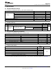
DRV2605L SLOS854C – MAY 2014 – REVISED SEPTEMBER 2014 www.ti.com Table of Contents 1 2 3 4 5 6 Features .................................................................. Applications ........................................................... Description ............................................................. Revision History..................................................... Pin Configuration and Functions ......................... Specifications.................................................
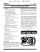
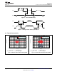
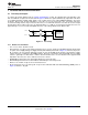
DRV2605L www.ti.com SLOS854C – MAY 2014 – REVISED SEPTEMBER 2014 5 Pin Configuration and Functions YZF Package 9-Pin DSBGA With 0,5-mm Pitch (Top View) A EN REG OUT+ B IN/TRIG SDA GND C SCL VDD OUT± 1 2 3 Pin Functions PIN TYPE (1) DESCRIPTION NO. NAME A1 EN I Device enable A2 REG O The REG pin is the 1.8-V regulator output. A 1-µF capacitor is required. A3 OUT+ O Positive haptic driver differential output B1 IN/TRIG I Multi-mode Input.
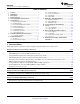
DRV2605L SLOS854C – MAY 2014 – REVISED SEPTEMBER 2014 www.ti.com DGS Package 10-Pin VSSOP (Top View) REG 1 10 SCL 2 9 OUT± SDA 3 8 GND IN/TRIG 4 7 OUT+ EN 5 6 VDD/NC VDD Pin Functions PIN NO. NAME TYPE (1) DESCRIPTION 1 REG O The REG pin is the 1.8-V regulator output. A 1-µF capacitor required 2 SCL I I2C clock 3 SDA I/O I2C data 4 IN/TRIG I Multi-mode Input. I2C selectable as PWM, analog, or trigger.
DRV2605L www.ti.com SLOS854C – MAY 2014 – REVISED SEPTEMBER 2014 6 Specifications 6.1 Absolute Maximum Ratings over operating free-air temperature range, TA = 25°C (unless otherwise noted) Input voltage MIN MAX UNIT VDD –0.3 5.5 V EN –0.3 VDD + 0.3 V SDA –0.3 VDD + 0.3 V SCL –0.3 VDD + 0.3 V IN/TRIG –0.3 VDD + 0.3 V Operating free-air temperature range, TA –40 85 °C Operating junction temperature range, TJ –40 150 °C 6.
DRV2605L SLOS854C – MAY 2014 – REVISED SEPTEMBER 2014 www.ti.com 6.5 Electrical Characteristics TA = 25°C, VDD = 3.6 V (unless otherwise noted) PARAMETER V(REG) TEST CONDITIONS MIN Voltage at the REG pin IIL Digital low-level input current IIH Digital high-level input current TYP MAX 1.83 UNIT V EN, IN/TRIG, SDA, SCL VDD = 5.2 V , VI = 0 V 1 IN/TRIG, SDA, SCL VDD = 5.2 V, VI = VDD 1 EN VDD = 5.2 V, VI = VDD 3.5 0.
DRV2605L www.ti.com SLOS854C – MAY 2014 – REVISED SEPTEMBER 2014 tw(H) tw(L) SCL tsu(1) th(1) SDA Figure 1. SCL and SDA Timing SCL tsu(2) tsu(3) th(2) t(BUF) SDA Start Condition Stop Condition Figure 2. Timing for Start and Stop Conditions 6.8 Typical Characteristics IN/TRIG Acceleration [OUT+] − [OUT−] (Filtered) Voltage (2V/div) Voltage (2V/div) IN/TRIG Acceleration [OUT+] − [OUT−] (Filtered) 0 40m VDD = 3.
DRV2605L SLOS854C – MAY 2014 – REVISED SEPTEMBER 2014 www.ti.com Typical Characteristics (continued) Voltage (2V/div) SDA Acceleration [OUT+] − [OUT−] (Filtered) Voltage (2V/div) SDA Acceleration [OUT+] − [OUT−] (Filtered) 0 200m 400m 600m Time (s) VDD = 3.6 V Sequence = 0x01, 0x48 800m 1 ERM open loop Internal trigger 0 200m 400m 600m Time (s) VDD = 3.6 V Transition click 1 - 100% Figure 5. ERM Click-Bounce (ROM) 800m 1 LRA closed loop Internal trigger Figure 6.
DRV2605L www.ti.com SLOS854C – MAY 2014 – REVISED SEPTEMBER 2014 7 Parameter Measurement Information 7.1 Test Setup for Graphs To capture the graphs displayed in the Typical Characteristics section, the following first-order RC-filter setup was used with the exception of the waveform in Figure 9 which was captured without any output filter. This filter is recommended when viewing output signals on an oscilloscope because output PWM modulation is present in all modes.
DRV2605L SLOS854C – MAY 2014 – REVISED SEPTEMBER 2014 www.ti.com 8 Detailed Description 8.1 Overview The DRV2605L device is a low-voltage haptic driver that relies on the back-EMF produced by an actuator to provide a closed-loop system that offers extremely flexible control of LRA and ERM actuators over a shared I2Ccompatible bus or PWM input signal. This schema helps improve actuator performance in terms of acceleration consistency, start time, and brake time.
DRV2605L www.ti.com SLOS854C – MAY 2014 – REVISED SEPTEMBER 2014 8.3 Feature Description 8.3.1 Support for ERM and LRA Actuators The DRV2605L device supports both ERM and LRA actuators. The ERM_LRA bit in register 0x1A must be configured to select the type of actuator that the device uses. 8.3.2 Smart-Loop Architecture The smart-loop architecture is an advanced closed-loop system that optimizes the performance of the actuator and allows for failure detection.
DRV2605L SLOS854C – MAY 2014 – REVISED SEPTEMBER 2014 www.ti.com Feature Description (continued) An open-loop haptic system typically drives an overdrive voltage at startup that is higher than the steady-state rated voltage of the actuator to decrease the startup latency of the actuator. Likewise, a braking algorithm must be employed for effective braking. When using an open-loop driver, these behaviors must be contained in the input waveform data.
DRV2605L www.ti.com SLOS854C – MAY 2014 – REVISED SEPTEMBER 2014 Feature Description (continued) 8.3.2.5 Automatic Level Calibration The smart-loop architecture uses actuator feedback by monitoring the back-EMF behavior of the actuator. The level of back-EMF voltage can vary across actuator manufacturers because of the specific actuator construction.
DRV2605L SLOS854C – MAY 2014 – REVISED SEPTEMBER 2014 www.ti.com Feature Description (continued) 8.3.3 Open-Loop Operation for LRA In the event that open-loop operation is desired (such as for off-resonance driving) the DRV2605L device includes an open-loop LRA drive mode that is available through the PWM input or through the digital interface.
DRV2605L www.ti.com SLOS854C – MAY 2014 – REVISED SEPTEMBER 2014 Feature Description (continued) Table 1. ERM Library Table (continued) LIBRARY RATED VOLTAGE OVERDRIVE VOLTAGE RISE TIME BRAKE TIME E 3V 3V > 140 ms > 30 ms F 4.5 V 5V 35 ms to 45 ms 10 ms to 20 ms 8.3.5.2.1 Waveform Sequencer The waveform sequencer queues waveform identifiers for playback. Eight sequence registers queue up to eight waveforms for sequential playback.
DRV2605L SLOS854C – MAY 2014 – REVISED SEPTEMBER 2014 www.ti.com For the LRA, the DRV2605L device automatically tracks the resonance frequency unless the LRA_OPEN_LOOP bit is set (in register 0x1D). If the LRA_OPEN_LOOP bit is set, the LRA is driven according to the open-loop frequency set in the OL_LRA_PERIOD[6:0] bit in register 0x20. 8.3.5.4 Analog Input Interface When the DRV2605L device is in analog-input interface mode, it accepts an analog voltage at the IN/TRIG pin.
DRV2605L www.ti.com SLOS854C – MAY 2014 – REVISED SEPTEMBER 2014 Edge Trigger Haptic Waveform Edge Trigger Cancellation Haptic Waveform Figure 14. Edge Trigger Mode 8.3.5.6.3 Level Trigger The actions of the GO bit directly follow the IN/TRIG pin. When the IN/TRIG pin is high, the GO bit is high. When the IN/TRIG pin goes low, the GO bit clears. Therefore, a falling edge cancels the transaction.
DRV2605L SLOS854C – MAY 2014 – REVISED SEPTEMBER 2014 www.ti.com 8.3.8 Battery Voltage Reporting During playback, the DRV2605L device provides real-time voltage measurement of the VDD pin. The VBAT[7:0] bit located in register 0x21 provides this information. 8.3.9 One-Time Programmable (OTP) Memory for Configuration The DRV2605L device contains nonvolatile, on-chip, OTP memory for specific configuration parameters.
DRV2605L www.ti.com SLOS854C – MAY 2014 – REVISED SEPTEMBER 2014 Case 1 Case 3 Case 2 Case 4 VDD VDD Return to default state Unknown state Return to default state Unknown state 2V 1.8 V REG V(BOT) 0V Time Slew rate > 3.6 kV/s Slew rate < 3.6 kV/s Slew rate < 3.6 kV/s Slew rate > 3.6 kV/s Figure 16. Brownout Behavior 8.4 Device Functional Modes 8.4.1 Power States The DRV2605L device has three different power states which allow for different power-consumption levels and functions.
DRV2605L SLOS854C – MAY 2014 – REVISED SEPTEMBER 2014 www.ti.com Device Functional Modes (continued) 8.4.1.4 Operation With STANDBY Control The STANDBY bit in register 0x01 forces the device in an out of the standby state. The STANDBY bit is asserted by default. When the STANDBY bit is asserted, the DRV2605L device goes into a low-power state. In the standby state the device retains register values and the ability to have I2C communication.
DRV2605L www.ti.com SLOS854C – MAY 2014 – REVISED SEPTEMBER 2014 8.4.3 Operation of the GO Bit The GO bit is the primary way to assert the GO signal, which fires processes in the DRV2605L device. The primary purpose of the GO bit is to fire the playback of the waveform identifiers in the waveform sequencer (registers 0x04 to 0x0B). However, The GO bit can also fire the calibration or diagnostics processes.
DRV2605L SLOS854C – MAY 2014 – REVISED SEPTEMBER 2014 www.ti.com 8.5 Programming 8.5.1 Auto-Resonance Engine Programming for the LRA 8.5.1.1 Drive-Time Programming The resonance frequency of each LRA actuator varies based on many factors and is generally dominated by mechanical properties. The auto-resonance engine-tracking system is optimized by providing information about the resonance frequency of the actuator. The DRIVE_TIME[4:0] bit is used as an initial guess for the half-period of the LRA..
DRV2605L www.ti.com SLOS854C – MAY 2014 – REVISED SEPTEMBER 2014 Programming (continued) 8.5.2.2 Overdrive Voltage-Clamp Programming During closed-loop operation, the actuator feedback allows the output voltage go above the rated voltage during the automatic overdrive and automatic braking periods. The OD_CLAMP[7:0] bit (in Register 0x17) sets a clamp so that the automatic overdrive is bounded. The OD_CLAMP[7:0] bit also serves as the full-scale reference voltage for open-loop operation.
DRV2605L SLOS854C – MAY 2014 – REVISED SEPTEMBER 2014 www.ti.com Programming (continued) 7-bit slave address R/W A b7 b6 b5 b4 b3 b2 b 1 b 0 8-bit register data for address (N) A 8-bit register address (N) b7 b6 b5 b4 b3 b2 b1 b0 b7 b6 b5 b4 b3 b2 b1 b0 A 8-bit register data for address (N) A b7 b6 b5 b4 b3 b2 b1 b0 Start Stop Figure 20. Typical I2C Sequence The DRV2605L device operates as an I2C-slave 1.8-V logic thresholds, but can operate up to the VDD voltage.
DRV2605L www.ti.com SLOS854C – MAY 2014 – REVISED SEPTEMBER 2014 Programming (continued) 8.5.3.4 Multiple-Byte Write and Incremental Multiple-Byte Write A multiple-byte data write transfer is identical to a single-byte data write transfer except that multiple data bytes are transmitted by the master device to the DRV2605L device as shown in Figure 22. After receiving each data byte, the DRV2605L device responds with an acknowledge bit.
DRV2605L SLOS854C – MAY 2014 – REVISED SEPTEMBER 2014 www.ti.com Programming (continued) 8.5.4 Programming for Open-Loop Operation The DRV2605L device can be used in open-loop mode and closed-loop mode. If open-loop operation is desired, the first step is to determine which actuator type is to use, either ERM or LRA. 8.5.4.
DRV2605L www.ti.com SLOS854C – MAY 2014 – REVISED SEPTEMBER 2014 Programming (continued) The following instructions list the step-by-step register configuration for auto-calibration. For additional details see the Register Map section. 1. Apply the supply voltage to the DRV2605L device, and pull the EN pin high. The supply voltage should allow for adequate drive voltage of the selected actuator. 2. Write a value of 0x07 to register 0x01.
DRV2605L SLOS854C – MAY 2014 – REVISED SEPTEMBER 2014 www.ti.com Programming (continued) 8.5.8 Waveform Playback Programming 8.5.8.1 Data Formats for Waveform Playback The DRV2605L smart-loop architecture has three modes of operation. Each of these modes can drive either ERM or LRA devices. 1. Open-loop mode 2. Closed-loop mode (unidirectional) 3. Closed-loop mode (bidirectional) Each mode has different advantages and disadvantages.
DRV2605L www.ti.com SLOS854C – MAY 2014 – REVISED SEPTEMBER 2014 Programming (continued) 8.5.8.1.2 Closed-Loop Mode, Unidirectional In closed-loop unidirectional mode, the DRV2605L device provides automatic overdrive and braking for both ERM and LRA devices. This mode is the most easy mode to use and understand. This mode uses the full 8-bit resolution of the driver.
DRV2605L SLOS854C – MAY 2014 – REVISED SEPTEMBER 2014 www.ti.com Programming (continued) 8.5.8.1.3 Closed-Loop Mode, Bidirectional In closed-loop bidirectional mode, the DRV2605L device provides automatic overdrive and braking for both ERM and LRA devices. This mode preserves compatibility with data created in open-loop signaling by maintaining zero drive-strength at the mid-scale value.
DRV2605L www.ti.com SLOS854C – MAY 2014 – REVISED SEPTEMBER 2014 Programming (continued) 8.5.8.2 Waveform Setup and Playback Playback of a haptic effect can occur in multiple ways. Using the PWM mode, RTP mode, audio-to-vibe mode, and analog-input mode can provide the waveform in real time. The waveforms can also be played from the ROM in which case the waveform playback engine is used and the waveform is either played by an internal GO bit (register 0x0C), or by an external trigger. 8.5.8.2.
DRV2605L SLOS854C – MAY 2014 – REVISED SEPTEMBER 2014 www.ti.com Programming (continued) GO Waveform Sequencer ROM Library WAV_FRM_SEQ0[7:0] Effect 1 WAV_FRM_SEQ1[7:0] Effect 2 WAV_FRM_SEQ2[7:0] Effect 3 WAV_FRM_SEQ3[7:0] Effect 4 WAV_FRM_SEQ4[7:0] Effect 5 WAV_FRM_SEQ5[7:0] WAV_FRM_SEQ6[7:0] WAV_FRM_SEQ7[7:0] Effect 123 Figure 29. Waveform Sequencer Programming 8.5.8.2.
DRV2605L www.ti.com SLOS854C – MAY 2014 – REVISED SEPTEMBER 2014 8.6 Register Map Table 3. Register Map Overview REG NO.
DRV2605L SLOS854C – MAY 2014 – REVISED SEPTEMBER 2014 www.ti.com 8.6.1 Status (Address: 0x00) Figure 30. Status Register 7 RO-1 6 DEVICE_ID[2:0] RO-1 5 4 Reserved RO-1 3 DIAG_RESULT RO-0 2 Reserved 1 OVER_TEMP RO-0 0 OC_DETECT RO-0 Table 4. Status Register Field Descriptions BIT FIELD TYPE DEFAULT DESCRIPTION 7-5 DEVICE_ID[2:0] RO 7 Device identifier. The DEVICE_ID bit indicates the part number to the user. The user software can ascertain the device capabilities by reading this register.
DRV2605L www.ti.com SLOS854C – MAY 2014 – REVISED SEPTEMBER 2014 8.6.2 Mode (Address: 0x01) Figure 31. Mode Register 7 DEV_RESET R/W-0 6 STANDBY R/W-1 5 4 Reserved 3 2 1 MODE[2:0] R/W-0 0 Table 5. Mode Register Field Descriptions BIT FIELD TYPE DEFAULT DESCRIPTION 7 DEV_RESET R/W 0 Device reset. Setting this bit performs the equivalent operation of power cycling the device. Any playback operations are immediately interrupted, and all registers are reset to the default values.
DRV2605L SLOS854C – MAY 2014 – REVISED SEPTEMBER 2014 www.ti.com 8.6.3 Real-Time Playback Input (Address: 0x02) Figure 32. Real-Time Playback Input Register 7 6 5 4 3 RTP_INPUT[7:0] R/W-0 2 1 0 Table 6. Real-Time Playback Input Register Field Descriptions BIT FIELD TYPE DEFAULT DESCRIPTION 7-0 RTP_INPUT[7:0] R/W 0 This field is the entry point for real-time playback (RTP) data. The DRV2605L playback engine drives the RTP_INPUT[7:0] value to the load when MODE[2:0] = 5 (RTP mode).
DRV2605L www.ti.com SLOS854C – MAY 2014 – REVISED SEPTEMBER 2014 8.6.5 Waveform Sequencer (Address: 0x04 to 0x0B) Figure 34. Waveform Sequencer Register 7 WAIT R/W-0 6 5 4 3 WAV_FRM_SEQ[6:0] R/W-0 2 1 0 Table 8. Waveform Sequencer Register Field Descriptions BIT FIELD TYPE DEFAULT DESCRIPTION 7 WAIT R/W 0 When this bit is set, the WAV_FRM_SEQ[6:0] bit is interpreted as a wait time in which the playback engine idles.
DRV2605L SLOS854C – MAY 2014 – REVISED SEPTEMBER 2014 www.ti.com 8.6.7 Overdrive Time Offset (Address: 0x0D) Figure 36. Overdrive Time Offset Register 7 6 5 4 3 2 1 0 ODT[7:0] R/W-0 Table 10. Overdrive Time Offset Register Field Descriptions BIT FIELD TYPE DEFAULT DESCRIPTION 7-0 ODT R/W 0 This bit adds a time offset to the overdrive portion of the library waveforms.
DRV2605L www.ti.com SLOS854C – MAY 2014 – REVISED SEPTEMBER 2014 8.6.9 Sustain Time Offset, Negative (Address: 0x0F) Figure 38. Sustain Time Offset, Negative Register 7 6 5 4 3 2 1 0 SNT[7:0] R/W-0 Table 12. Sustain Time Offset, Negative Register Field Descriptions BIT FIELD TYPE DEFAULT DESCRIPTION 7-0 SNT R/W 0 This bit adds a time offset to the negative sustain portion of the library waveforms.
DRV2605L SLOS854C – MAY 2014 – REVISED SEPTEMBER 2014 www.ti.com 8.6.11 Audio-to-Vibe Control (Address: 0x11) Figure 40. Audio-to-Vibe Control Register 7 6 5 4 3 2 ATH_PEAK_TIME[1:0] R/W-0 R/W-1 Reserved 1 0 ATH_FILTER[1:0] R/W-0 R/W-1 Table 14.
DRV2605L www.ti.com SLOS854C – MAY 2014 – REVISED SEPTEMBER 2014 8.6.14 Audio-to-Vibe Minimum Output Drive (Address: 0x14) Figure 43. Audio-to-Vibe Minimum Output Drive Register 7 6 5 R/W-0 R/W-0 R/W-0 4 3 ATH_MIN_DRIVE[7:0] R/W-1 R/W-1 2 1 0 R/W-0 R/W-0 R/W-1 Table 17. Audio-to-Vibe Minimum Output Drive Register Field Descriptions BIT FIELD TYPE DEFAULT DESCRIPTION 7-0 ATH_MIN_DRIVE[7:0] R/W 0x19 This bit sets the minimum output level that is applied to the actuator drive engine.
DRV2605L SLOS854C – MAY 2014 – REVISED SEPTEMBER 2014 www.ti.com 8.6.17 Overdrive Clamp Voltage (Address: 0x17) Figure 46. Overdrive Clamp Voltage Register 7 6 5 R/W-1 R/W-0 R/W-0 4 3 OD_CLAMP[7:0] R/W-1 R/W-1 2 1 0 R/W-1 R/W-0 R/W-0 Table 20.
DRV2605L www.ti.com SLOS854C – MAY 2014 – REVISED SEPTEMBER 2014 8.6.20 Feedback Control (Address: 0x1A) Figure 49. Feedback Control Register 7 N_ERM_LRA R/W-0 6 5 4 FB_BRAKE_FACTOR[2:0] R/W-0 R/W-1 R/W-1 3 2 LOOP_GAIN[1:0] R/W-0 R/W-1 1 0 BEMF_GAIN[1:0] R/W-1 R/W-0 Table 23. Feedback Control Register Field Descriptions BIT FIELD TYPE DEFAULT DESCRIPTION 7 N_ERM_LRA R/W 0 This bit sets the DRV2605L device in ERM or LRA mode. This bit should be set prior to running auto calibration.
DRV2605L SLOS854C – MAY 2014 – REVISED SEPTEMBER 2014 www.ti.com 8.6.21 Control1 (Address: 0x1B) Figure 50. Control1 Register 7 STARTUP_BO OST R/W-1 6 Reserved 5 AC_COUPLE 4 3 2 DRIVE_TIME[4:0] 1 0 R/W-0 R/W-1 R/W-0 R/W-0 R/W-1 R/W-1 Table 24. Control1 Register Field Descriptions BIT FIELD TYPE DEFAULT DESCRIPTION 7 STARTUP_BOOST R/W 1 This bit applies higher loop gain during overdrive to enhance actuator transient response. 6 Reserved 5 AC_COUPLE R/W 0 This bit applies a 0.
DRV2605L www.ti.com SLOS854C – MAY 2014 – REVISED SEPTEMBER 2014 8.6.22 Control2 (Address: 0x1C) Figure 51. Control2 Register 7 BIDIR_INPUT R/W-1 6 BRAKE_STABI LIZER R/W-1 5 4 SAMPLE_TIME[1:0] 3 2 BLANKING_TIME[1:0] R/W-1 R/W-0 1 0 IDISS_TIME[1:0] R/W-1 R/W-0 R/W-1 Table 25. Control2 Register Field Descriptions BIT FIELD TYPE DEFAULT DESCRIPTION 7 BIDIR_INPUT R/W 1 The BIDIR_INPUT bit selects how the engine interprets data.
DRV2605L SLOS854C – MAY 2014 – REVISED SEPTEMBER 2014 www.ti.com Table 25. Control2 Register Field Descriptions (continued) BIT FIELD TYPE DEFAULT DESCRIPTION 3-2 BLANKING_TIME[1:0] R/W 2 Blanking time before the back-EMF AD makes a conversion. (Advanced use only) Blanking time for LRA has an additional 2 bits (BLANKING_TIME[3:2]) located in register 0x1F. Depending on the status of N_ERM_LRA the blanking time represents different values.
DRV2605L www.ti.com SLOS854C – MAY 2014 – REVISED SEPTEMBER 2014 Table 25. Control2 Register Field Descriptions (continued) BIT FIELD TYPE DEFAULT DESCRIPTION 1-0 IDISS_TIME[1:0] R/W 2 Current dissipation time. This bit is the time allowed for the current to dissipate from the actuator between PWM cycles for flyback mitigation. (Advanced use only) the current dissipation time for LRA has an additional 2 bits (IDISS_TIME[3:2]) located in register 0x1F.
DRV2605L SLOS854C – MAY 2014 – REVISED SEPTEMBER 2014 www.ti.com 8.6.23 Control3 (Address: 0x1D) Figure 52. Control3 Register 7 6 NG_THRESH[1:0] R/W-1 R/W-0 5 ERM_OPEN_L OOP R/W-1 4 SUPPLY_COM P_DIS R/W-0 3 2 1 DATA_FORMA LRA_DRIVE_M N_PWM_ANAL T_RTP ODE OG R/W-0 R/W-0 R/W-0 0 LRA_OPEN_L OOP R/W-0 Table 26. Control3 Register Field Descriptions BIT 7-6 FIELD NG_THRESH[1:0] TYPE R/W DEFAULT 1 DESCRIPTION This bit is the noise-gate threshold for PWM and analog inputs.
DRV2605L www.ti.com SLOS854C – MAY 2014 – REVISED SEPTEMBER 2014 8.6.24 Control4 (Address: 0x1E) Figure 53. Control4 Register 7 6 ZC_DET_TIME[ ZC_DET_TIME[ 1] 0] R/W-0 R/W-0 5 4 AUTO_CAL_TIME[1:0] R/W-1 3 Reserved R/W-0 2 OTP_STATUS R-0 1 Reserved 0 OTP_PROGRA M R/W-0 Table 27. Control4 Register Field Descriptions BIT FIELD TYPE DEFAULT DESCRIPTION 7-6 ZC_DET_TIME[1:0] R/W 0 This bit sets the minimum length of time devoted for detecting a zero crossing (advanced use only).
DRV2605L SLOS854C – MAY 2014 – REVISED SEPTEMBER 2014 www.ti.com 8.6.25 Control5 (Address: 0x1F) Figure 54. Control5 Register 7 6 AUTO_OL_CNT[1:0] R/W-1 5 LRA_AUTO_O PEN_LOOP R/W-0 R/W-0 4 PLAYBACK_IN TERVAL R/W-0 3 2 BLANKING_TIME[3:2] RW-0 RW-0 1 0 IDISS_TIME[3:2] RW-0 Table 28.
DRV2605L www.ti.com SLOS854C – MAY 2014 – REVISED SEPTEMBER 2014 8.6.27 V(BAT) Voltage Monitor (Address: 0x21) Figure 56. V(BAT) Voltage-Monitor Register 7 6 5 4 3 2 1 0 VBAT[7:0] R/W-0 Table 30. V(BAT) Voltage-Monitor Register Field Descriptions BIT FIELD TYPE DEFAULT DESCRIPTION 7-0 VBAT[7:0] R/W 0 This bit provides a real-time reading of the supply voltage at the VDD pin. The device must be actively sending a waveform to take a reading. VDD (V) = VBAT[7:0] × 5.6V / 255 8.6.
DRV2605L SLOS854C – MAY 2014 – REVISED SEPTEMBER 2014 www.ti.com 9 Application and Implementation NOTE Information in the following applications sections is not part of the TI component specification, and TI does not warrant its accuracy or completeness. TI’s customers are responsible for determining suitability of components for their purposes. Customers should validate and test their design implementation to confirm system functionality. 9.
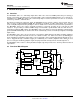
DRV2605L www.ti.com SLOS854C – MAY 2014 – REVISED SEPTEMBER 2014 9.2 Typical Application A typical application of the DRV2605L device is in a system that has external buttons which fire different haptic effects when pressed. Figure 60 shows a typical schematic of such a system. The buttons can be physical buttons, capacitive-touch buttons, or GPIO signals coming from the touch-screen system. Effects in this type of system are programmable. TPS73633 OUT NR/FB IN EN GND C (LDO) 1 µF R (PU) 2.
DRV2605L SLOS854C – MAY 2014 – REVISED SEPTEMBER 2014 www.ti.com IL IL OUT+ OUT+ + Motor-spin direction ± Motor-spin direction VO VO + ± OUT± OUT± IL IL Figure 61. Motor Spin Direction in ERM Motors Another common approach to driving DC motors is the concept of overdrive voltage. To overcome the inertia of the mass of the motor, these motors are often overdriven for a short amount of time before returning to the rated voltage of the motor to sustain the rotation of the motor.
DRV2605L www.ti.com SLOS854C – MAY 2014 – REVISED SEPTEMBER 2014 9.2.2.3 Interface Selection The I2C interface is required to configure the device. The device can be used fully with this interface and with either RTP or internal memory. The advantage of using this interface is that no additional GPIO (for the IN/TRIG pin) is required for firing effects, and no PWM signal is required to be generated. Therefore the IN/TRIG pin can be connected to GND.
DRV2605L SLOS854C – MAY 2014 – REVISED SEPTEMBER 2014 www.ti.com 9.3 Initialization Setup 9.3.1 Initialization Procedure 1. 2. 3. 4. 5. 6. 7. 8. After powerup, wait at least 250 µs before the DRV2605L device accepts I2C commands. Assert the EN pin (logic high). The EN pin can be asserted any time during or after the 250 µs wait period. Write the MODE register (address 0x01) to value 0x00 to remove the device from standby mode.
DRV2605L www.ti.com SLOS854C – MAY 2014 – REVISED SEPTEMBER 2014 Initialization Setup (continued) 9.3.2.3 Play a PWM or Analog Input Waveform 1. Initialize the device as shown in the Initialization Procedure section. 2. Assert the EN pin (active high) if it was previously deasserted. 3. If register 0x01 already holds the desired value and the STANDBY bit is low, the user can skip this step. Set the MODE value to 3 (PWM/Analog Mode) at address 0x01.
DRV2605L SLOS854C – MAY 2014 – REVISED SEPTEMBER 2014 www.ti.com 11 Layout 11.1 Layout Guidelines Use the following guidelines for the DRV2605L layout: • The decoupling capacitor for the power supply (VDD) should be placed closed to the device pin. • The filtering capacitor for the regulator (REG) should be placed close to the device REG pin. • When creating the pad size for the WCSP pins, TI recommends that the PCB layout use nonsolder maskdefined (NSMD) land.
DRV2605L www.ti.com SLOS854C – MAY 2014 – REVISED SEPTEMBER 2014 11.1.1 Trace Width The recommended trace width at the solder pins is 75 µm to 100 µm to prevent solder wicking onto wider PCB traces. Maintain this trace width until the pin pattern is escaped then the trace width can be increased for improved current flow. The width and length of the 75-µm to 100-µm traces should be as symmetrical as possible around the device to provide even solder reflow on each of the pins. 11.
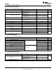
DRV2605L SLOS854C – MAY 2014 – REVISED SEPTEMBER 2014 www.ti.com 12 Device and Documentation Support 12.1 Device Support 12.1.
DRV2605L www.ti.com SLOS854C – MAY 2014 – REVISED SEPTEMBER 2014 Device Support (continued) EFFECT ID NO. WAVEFORM NAME EFFECT ID NO> WAVEFORM NAME EFFECT ID NO.
PACKAGE OPTION ADDENDUM www.ti.
PACKAGE OPTION ADDENDUM www.ti.com 1-Oct-2014 Important Information and Disclaimer:The information provided on this page represents TI's knowledge and belief as of the date that it is provided. TI bases its knowledge and belief on information provided by third parties, and makes no representation or warranty as to the accuracy of such information. Efforts are underway to better integrate information from third parties.
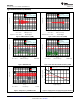
PACKAGE MATERIALS INFORMATION www.ti.com 17-Jun-2015 TAPE AND REEL INFORMATION *All dimensions are nominal Device DRV2605LDGSR Package Package Pins Type Drawing VSSOP DGS 10 DRV2605LDGST VSSOP DGS DRV2605LYZFR DSBGA YZF DRV2605LYZFT DSBGA YZF SPQ Reel Reel A0 Diameter Width (mm) (mm) W1 (mm) K0 (mm) P1 (mm) W Pin1 (mm) Quadrant 3.4 1.4 8.0 12.0 Q1 2500 330.0 12.4 10 250 330.0 12.4 5.3 3.4 1.4 8.0 12.0 Q1 9 3000 180.0 8.4 1.65 1.65 0.81 4.0 8.
PACKAGE MATERIALS INFORMATION www.ti.com 17-Jun-2015 *All dimensions are nominal Device Package Type Package Drawing Pins SPQ Length (mm) Width (mm) Height (mm) DRV2605LDGSR VSSOP DGS 10 2500 366.0 364.0 50.0 DRV2605LDGST VSSOP DGS 10 250 366.0 364.0 50.0 DRV2605LYZFR DSBGA YZF 9 3000 182.0 182.0 20.0 DRV2605LYZFT DSBGA YZF 9 250 182.0 182.0 20.
D: Max = 1.47 mm, Min = 1.41 mm E: Max = 1.47 mm, Min = 1.
IMPORTANT NOTICE Texas Instruments Incorporated and its subsidiaries (TI) reserve the right to make corrections, enhancements, improvements and other changes to its semiconductor products and services per JESD46, latest issue, and to discontinue any product or service per JESD48, latest issue. Buyers should obtain the latest relevant information before placing orders and should verify that such information is current and complete.